GENERAL DESCRIPTION
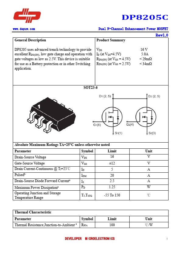
Dual N-Channel Enhancement Power MOSFET Product Summary Rev1.0 DP8205 uses advanced trench technology to provide excellent RDS(ON), low gate charge and operation with gate voltages as low as 2.5V. VDS ID (at VGS=4.5V) RDS(ON) (at VGS = 4.5V) RDS(ON) (at VGS = 2.5V) 16 V 5.0A < 29mΩ < 34mΩ SOT23-6 ABSOLUTE MAXIMUM RATINGS
TA=25°C unless otherwise noted Parameter Drain-Source Voltage Gate-Source Voltage Drain Current-Continuous @ TJ=25℃ Pulsedb Drain-Sourse Diode Forward Currenta Maximum Power Dissipationa Operating Junction and Storage Temperature Range Symbol VDS VGS ID IDM IS PD TJ,TSTG Limit 16 ±12 5 20 2.5 1.25 -55 To 150 Thermal Characteristic Parameter Thermal Resistance,Junction-to-Ambient a Symbol RθJA Limit 100 DEVELOPER MICROELECTRONICS Unit V V A A A W ℃ Unit ℃/W 1