Datasheet4U Logo Datasheet4U.com

74HCT595S16 - 8-BIT SHIFT REGISTER

Download the 74HCT595S16 datasheet PDF. This datasheet also covers the 74HCT595 variant, as both devices belong to the same 8-bit shift register family and are provided as variant models within a single manufacturer datasheet.

General Description

The 74HCT595 is an high speed CMOS device that is designed to be pin compatable with 74LS low power Schottky types.

An eight bit shift register accpets data from the serial input (DS) on each positive transition of the shift register clock (STCP).

Key Features

  • Supply Voltage Range from 4.5V to 5.5V.
  • Sinks or sources 8mA at VCC = 4.5V.
  • CMOS low power consumption.
  • Schmitt Trigger Action at All Inputs.
  • Inputs accept up to 6.0V.
  • ESD Protection Tested per JESD 22 Exceeds 200-V Machine Model (A115-A) Exceeds 2000-V Human Body Model (A114-A) Exceeds 1000-V Charged Device Model (C101C).
  • Latch-Up Exceeds 250mA per JESD 78, Class II.
  • Totally Lead-Free & Fully RoHS Compliant (Notes 1 & 2).

📥 Download Datasheet

Note: The manufacturer provides a single datasheet file (74HCT595-Diodes.pdf) that lists specifications for multiple related part numbers.

Full PDF Text Transcription (Reference)

The following content is an automatically extracted verbatim text from the original manufacturer datasheet and is provided for reference purposes only.

View original datasheet text
Preliminary 74HCT595 8-BIT SHIFT REGISTER WITH 8-BIT OUTPUT REGISTER Description 
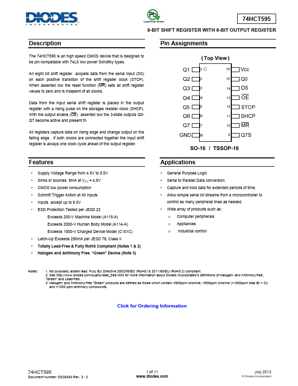
Pin Assignments The 74HCT595 is an high speed CMOS device that is designed to be pin compatable with 74LS low power Schottky types. An eight bit shift register accpets data from the serial input (DS) on each positive transition of the shift register clock (STCP). When asserted low the reset function (MR) sets all shift register values to zero and is indepent of all clocks. Data from the input serial shift register is placed in the output register with a rising pulse on the storages resister clock (SHCP). With the output enable (OEሻ asserted low the 3-state outputs Q0Q7 become active and present th All registers capture data on rising edge and change output on the falling edge.