PI6CB184Q
PI6CB184Q is 4-Output PCIe Gen 4 Clock Buffer manufactured by Diodes Incorporated.
Pb
Lead-free Green
A product Line of Diodes Incorporated
4-Output PCIe Gen 4 Clock Buffer for Automotive Applications
Features
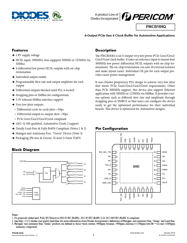
ÎÎ1.8V supply voltage ÎÎHCSL input: 100MHz, also suppport 50MHz or 125MHz via
SMBus ÎÎ4 differential low power HCSL outputs with on-chip termination ÎÎIndividual output enable ÎÎProgrammable Slew rate and output amplitute for each output ÎÎDifferential outputs blocked until PLL is locked ÎÎStrapping pins or SMBus for configuration; ÎÎ3.3V tolerant SMBus interface support ÎÎVery low jitter outputs yyDifferential cycle-to-cycle jitter <50ps yyDifferential output-to-output skew <50ps yyPCIe Gen1/Gen2/Gen3/Gen4 pliant ÎÎAEC-Q 100 qualified, Automotive...