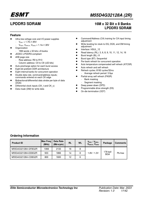
M55D4G32128A-CDBG2R
M55D4G32128A-CDBG2R is 16M x 32 Bit x 8 Banks LPDDR3 SDRAM manufactured by Elite Semiconductor Microelectronics Technology.
- Part of the M55D4G32128A-GFBG2R comparator family.
- Part of the M55D4G32128A-GFBG2R comparator family.
ESMT
LPDDR3 SDRAM
Feature
- Ultra-low-voltage core and I/O power supplies VDD1 = 1.70- 1.95V VDD2, VDDCA, VDDQ = 1.14- 1.30V
- Organization 16M words x 32 bits x 8 banks
- JEDEC LPDDR3-pliant
- 4KB page size
Row address: R0 to R13 Column address: C0 to C9 (x32 bits)
- Auto precharge option for each burst access
- Eight-bit prefetch DDR architecture
- Eight internal banks for concurrent operation
- Double data rate, mand/address inputs; mands entered on each CK edge
- Bidirectional/differential data strobe per byte of data (DQS)
- Differential clock inputs (CK_t and CK_c)
- Data mask (DM) for write data
M55D4G32128A (2R)
16M x 32 Bit x 8 Banks LPDDR3 SDRAM
-...