Datasheet Details
| Part number | EDD2504AKTA |
|---|---|
| Manufacturer | Elpida Memory |
| File Size | 492.04 KB |
| Description | 256M bits DDR SDRAM (64M words x 4 bits) |
| Datasheet |
 EDD2504AKTA Datasheet EDD2504AKTA Datasheet
|
|
|
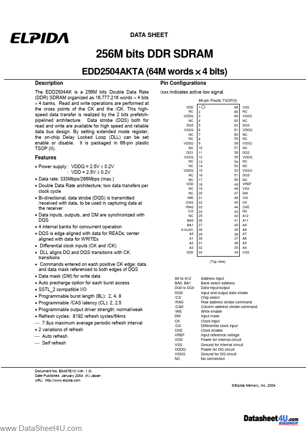
The EDD2504AK is a 256M bits Double Data Rate (DDR) SDRAM organized as 16,777,216 words × 4 bits × 4 banks.
Read and write operations are performed at the cross points of the CK and the /CK.
This highspeed data transfer is realized by the 2 bits prefetchpipelined architecture.
| Part number | EDD2504AKTA |
|---|---|
| Manufacturer | Elpida Memory |
| File Size | 492.04 KB |
| Description | 256M bits DDR SDRAM (64M words x 4 bits) |
| Datasheet |
EDD2504AKTA Datasheet
|
|
|
|
| Part Number | Description | Manufacturer |
|---|---|---|
| EDD11 | Doppelendtriode | TELEFUNKEN |
| Part Number | Description |
|---|---|
| EDD2504AKTA | 256M bits DDR SDRAM (64M words x 4 bits) |
| EDD2504AKTA-E | 256M bits DDR SDRAM (64M words x 4 bits) |
| EDD2504AKTA-E | 256M bits DDR SDRAM (64M words x 4 bits) |
| EDD2508AETA | (EDD2508AETA / EDD2516AETA) 256M bits DDR SDRAM |
| EDD2508AKTA-5 | 256M bits DDR SDRAM (32M words x 8 bits DDR400) |
The following content is an automatically extracted verbatim text from the original manufacturer datasheet and is provided for reference purposes only.