Datasheet4U Logo Datasheet4U.com

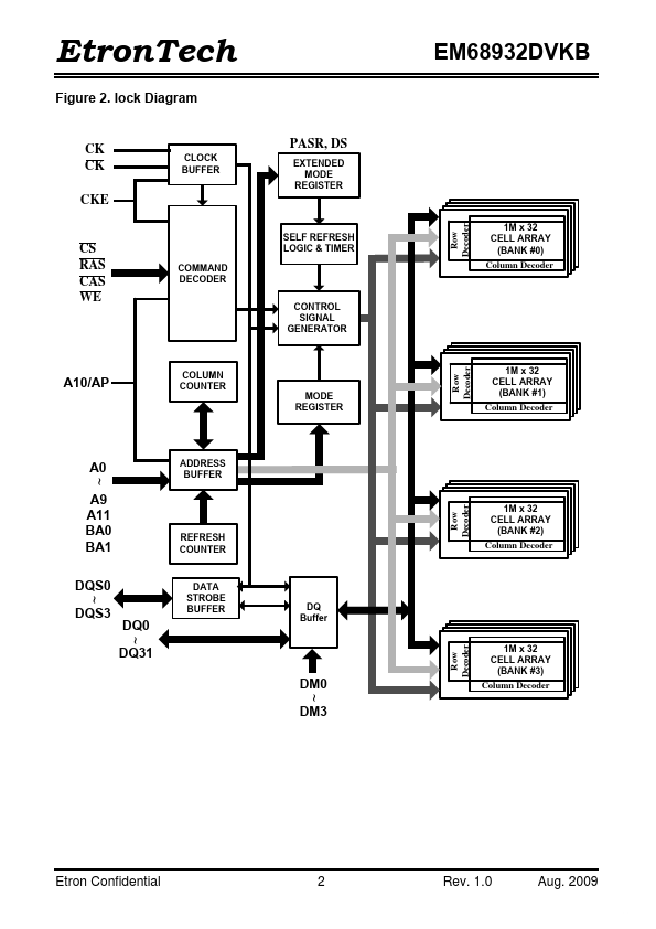
EM68932DVKB - 4M x 32 Mobile DDR Synchronous DRAM

Description

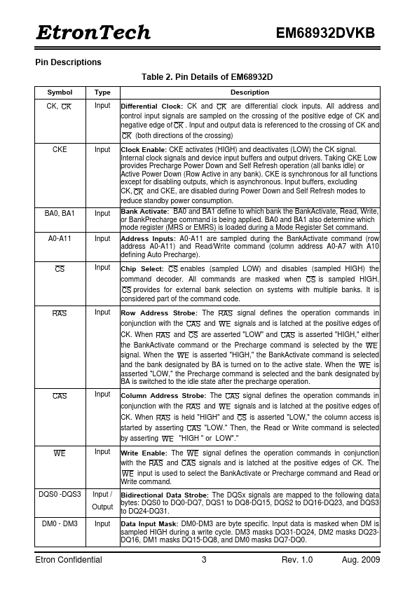
Table 2.

Differential Clock: CK and CK are differential clock inputs.

All address and control input signals are sampled on the crossing of the positive edge of CK and negative edge of CK .

Features

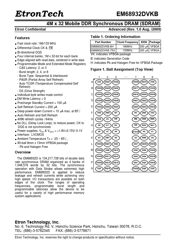
  • Fast clock rate: 166/133 MHz Differential Clock CK & CK Bi-directional DQS Four internal banks, 1M x 32-bit for each bank Edge-aligned with read data, centered in write data Programmable Mode and Extended Mode Registers - CAS Latency: 2, or 3 - Burst length: 2, 4, or 8 - Burst Type: Sequential & Interleaved - PASR (Partial Array Self Refresh) - Auto TCSR (Temperature Compensated Self Refresh) - DS (Drive Strength).
  • Individual byte writes mask control.
  • DM Write Latency = 0.

📥 Download Datasheet

Datasheet Details

Part number EM68932DVKB
Manufacturer Etron Technology
File Size 444.58 KB
Description 4M x 32 Mobile DDR Synchronous DRAM
Datasheet download datasheet EM68932DVKB Datasheet
Other Datasheets by Etron Technology

Full PDF Text Transcription

Click to expand full text
www.DataSheet.co.kr EtronTech Etron Confidential Features Fast clock rate: 166/133 MHz Differential Clock CK & CK Bi-directional DQS Four internal banks, 1M x 32-bit for each bank Edge-aligned with read data, centered in write data Programmable Mode and Extended Mode Registers - CAS Latency: 2, or 3 - Burst length: 2, 4, or 8 - Burst Type: Sequential & Interleaved - PASR (Partial Array Self Refresh) - Auto TCSR (Temperature Compensated Self Refresh) - DS (Drive Strength) • Individual byte writes mask control • DM Write Latency = 0 • Precharge Standby Current = 100 µA • Self Refresh Current = 200 µA • Deep power-down Current = 10 µA max. at 85℃ • Auto Refresh and Self Refresh • 4096 refresh cycles / 64ms • No DLL (Delay Lock Loop), to reduce power; CK to DQS is not synchronized.
Published: |