EMD02N06TL8
EMD02N06TL8 is Single N-Channel Logic Level Enhancement Mode Field Effect Transistor manufactured by Excelliance MOS.
Single N-Channel Logic Level Enhancement Mode Field Effect Transistor
- Product Summary:
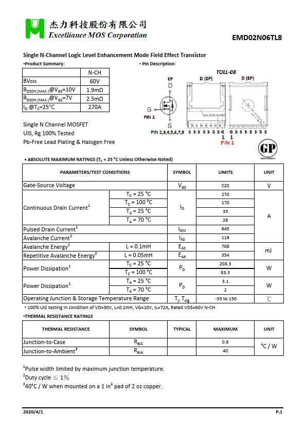
- Pin Description:
N-CH
BVDSS
60V
RDSON (MAX.)@VGS=10V RDSON (MAX.)@VGS=7V ID @TC=25℃
1.9mΩ 2.5mΩ 270A
Single N Channel MOSFET UIS, Rg 100% Tested Pb-Free Lead Plating & Halogen Free
-...