Datasheet Details
| Part number | 74LCX112 |
|---|---|
| Manufacturer | Fairchild Semiconductor (now onsemi) |
| File Size | 124.96 KB |
| Description | Low Voltage Dual J-K Negative Edge-Triggered Flip-Flop |
| Datasheet |
 74LCX112 Datasheet 74LCX112 Datasheet
|
|
|
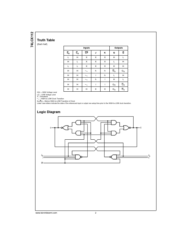
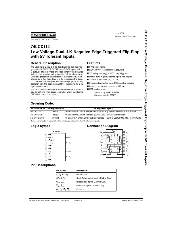
The LCX112 is a dual J-K flip-flop.
Each flip-flop has independent J, K, PRESET, CLEAR, and CLOCK inputs with Q, Q outputs.
These devices are edge sensitive and change state on the negative going transition of the clock pulse.
| Part number | 74LCX112 |
|---|---|
| Manufacturer | Fairchild Semiconductor (now onsemi) |
| File Size | 124.96 KB |
| Description | Low Voltage Dual J-K Negative Edge-Triggered Flip-Flop |
| Datasheet |
74LCX112 Datasheet
|
|
|
|