CD4007CN Overview
Key Specifications
Package: DIP
Operating Voltage: 5 V
Max Voltage (typical range): 15 V
Min Voltage (typical range): 3 V
Description
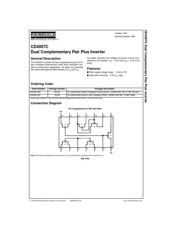
The CD4007C consists of three complementary pairs of Nand P-channel enhancement mode MOS transistors suitable for series/shunt applications. All inputs are protected from static discharge by diode clamps to VDD and VSS.
Key Features
- Specify by appending the suffix letter “X” to the ordering code
- Top View © 1999 Fairchild Semiconductor Corporation CD4007C