CD4027BCN Overview
Key Specifications
Package: DIP
Mount Type: Through Hole
Pins: 16
Operating Voltage: 5 V
Description
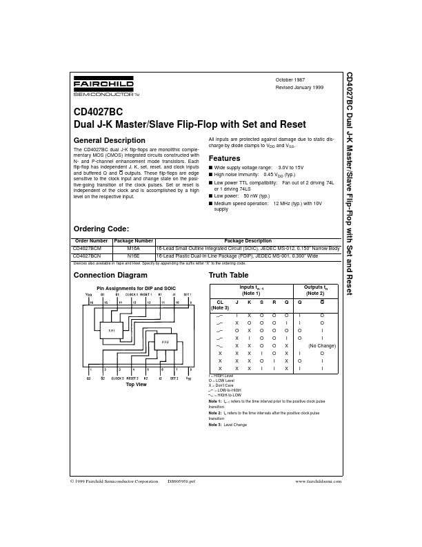
The CD4027BC dual J-K flip-flops are monolithic complementary MOS (CMOS) integrated circuits constructed with N- and P-channel enhancement mode transistors. Each flip-flop has independent J, K, set, reset, and clock inputs and buffered Q and Q outputs.
Key Features
- J I X O X X X X X K X O X I X X X X S O O O O O I O I R O O O O O O I I Q O I O I X X X X I O I Q I I O O Outputs tn (Note