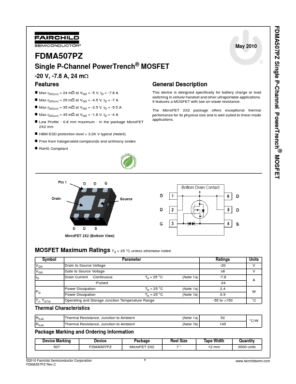
FDMA507PZ Overview
Description
This device is designed specifically for battery charge or load switching in cellular handset and other ultraportable applications. It features a MOSFET with low on-stade resistance.
Key Features
- Max rDS(on) = 24 mΩ at VGS = -5 V, ID = -7.8 A
- Max rDS(on) = 25 mΩ at VGS = -4.5 V, ID = -7 A
- Max rDS(on) = 35 mΩ at VGS = -2.5 V, ID = -5.5 A
- Max rDS(on) = 45 mΩ at VGS = -1.8 V, ID = -4 A
- 0.8 mm maximum
- in the package MicroFET 2X2 mm
- HBM ESD protection level > 3.2K V typical (Note3)
- Free from halogenated compounds and antimony oxides
- RoHS Compliant