Download FDS8949 Datasheet PDF
Fairchild Semiconductor
FDS8949
FDS8949 is Dual N-Channel MOSFET manufactured by Fairchild Semiconductor.
Features - Max r DS(on) = 29mΩ at VGS = 10V - Max r DS(on) = 36mΩ at VGS = 4.5V - Low gate charge - High performance trench technology for extremely low r DS(on) - High power and current handling capability - Ro HS pliant tm General Description 
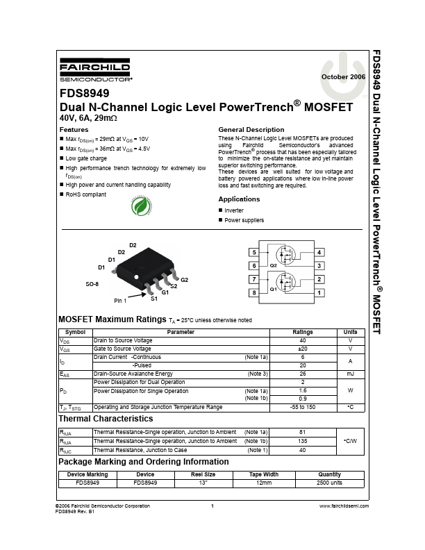
These N-Channel Logic Level MOSFETs are produced using Fairchild Semiconductor’s advanced Power Trench® process that has been especially tailored to minimize the on-state resistance and yet maintain superior switching performance. These devices are well suited for low voltage and battery powered applications where low in-line power loss and fast switching are required. Applications - Inverter - Power suppliers D2 D2 D1 D1 SO-8 Pin 1 S1 G1 G2 S2 MOSFET Maximum Ratings TA = 25°C unless otherwise noted Symbol VDS VGS ID EAS PD TJ, TSTG Parameter Drain to Source Voltage Gate to Source Voltage Drain Current -Continuous -Pulsed Drain-Source Avalanche Energy Power Dissipation for Dual Operation Power Dissipation for Single Operation Operating and Storage Junction Temperature Range (Note 1a) (Note 1b) (Note 3) (Note 1a) Ratings 40 ±20 6 20 26 2 1.6 0.9 -55 to 150 °C W Units V V A m J Thermal Characteristics RθJA RθJA RθJC Thermal Resistance-Single operation, Junction to Ambient Thermal Resistance-Single operation, Junction to Ambient Thermal Resistance, Junction to Case (Note 1a) (Note 1b) (Note 1) 81 135 40 °C/W Package Marking and Ordering Information Device Marking FDS8949 Device FDS8949 Reel Size 13’’ Tape Width 12mm Quantity 2500 units ©2006 Fairchild Semiconductor Corporation FDS8949 Rev. B1 .fairchildsemi. FDS8949 Dual N-Channel Logic Level Power Trench® MOSFET Electrical Characteristics TJ = 25°C unless otherwise noted Symbol Parameter Test Conditions Min Typ Max Units Off Characteristics BVDSS ∆BVDSS ∆TJ IDSS IGSS Drain to Source Breakdown Voltage ID = 250µA, VGS = 0V Breakdown Voltage Temperature Coefficient Zero Gate Voltage Drain Current Gate to Source Leakage Current ID = 250µA, referenced to 25°C VDS = 32V, VGS...