Datasheet4U Logo Datasheet4U.com

MCZ33689D - System Basis Chip

General Description

of each pin can be found in the Functional Pin Description section beginning on page 19.

7 8, 9, 24, 25 10 11 12 13 15 16 17 18 19 20 21 Pin Name NC L1, L2 HS3 HS1 TGND VS2 LIN GND VS1 VDD AGND VCC OUT EE+ WDC Formal Name No Connect Level Inputs 1 and 2 High-Si

Key Features

  • The device provide full SPI-readable diagnostics and a selectable timing watchdog for detecting errant operation. The LIN transceiver waveshaping circuitry can be disabled for higher data rates. One 50 mA and two 150 mA high-side switches with output protection are available to drive inductive or resistive loads. The 150 mA switches can be pulse-width modulated (PWM). Two high-voltage inputs are available for contact monitoring or as external wake-up inputs. A current sense operational amplifie.

📥 Download Datasheet

Full PDF Text Transcription for MCZ33689D (Reference)

Note: Below is a high-fidelity text extraction (approx. 800 characters) for MCZ33689D. For precise diagrams, and layout, please refer to the original PDF.

www.DataSheet4U.com 
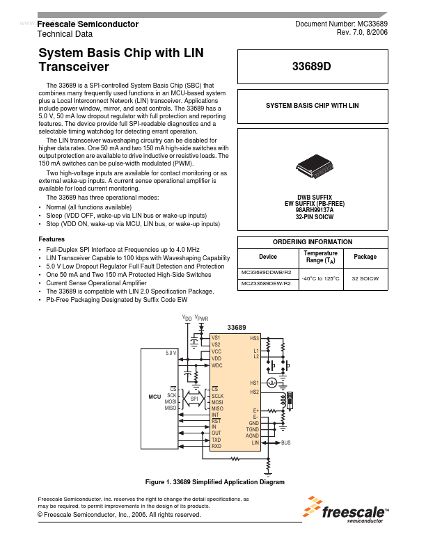
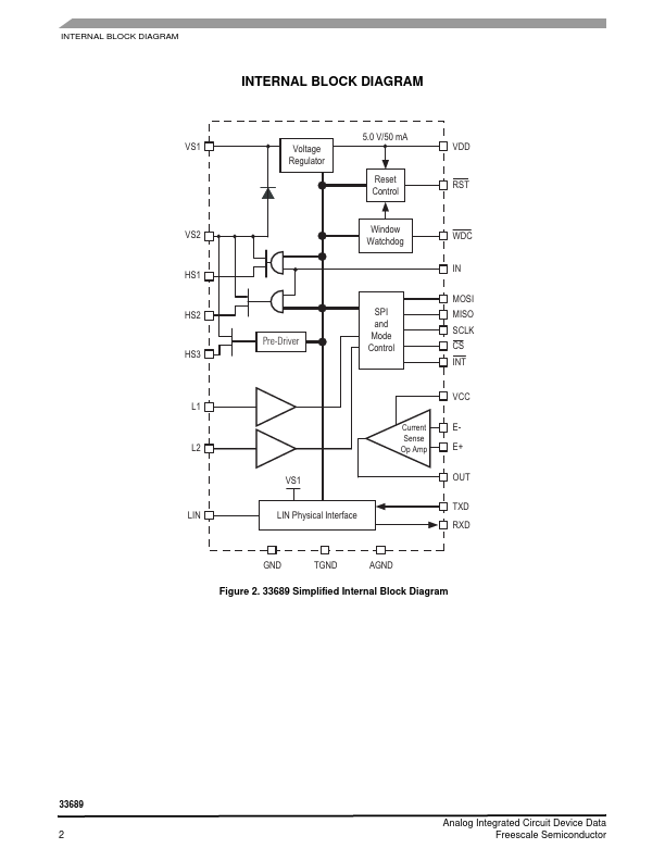
Freescale Semiconductor Technical Data Document Number: MC33689 Rev. 7.0, 8/2006 System Basis Chip with LIN Transceiver The 33689 is a SPI-controlled ...

View more extracted text
System Basis Chip with LIN Transceiver The 33689 is a SPI-controlled System Basis Chip (SBC) that combines many frequently used functions in an MCU-based system plus a Local Interconnect Network (LIN) transceiver. Applications include power window, mirror, and seat controls. The 33689 has a 5.0 V, 50 mA low dropout regulator with full protection and reporting features. The device provide full SPI-readable diagnostics and a selectable timing watchdog for detecting errant operation. The LIN transceiver waveshaping circuitry can be disabled for higher data rates. One 50 mA and two 150 mA high-side switches with output protec