MCZ33661
MCZ33661 is Local Area Network (LIN) Enhanced Physical Interface manufactured by Freescale Semiconductor.
.. Freescale Semiconductor
Advance Information
Document Number: MC33661 Rev. 6.0, 11/2006
Local Area Network (LIN) Enhanced Physical Interface with Selectable Slew Rate
Local Interconnect Network (LIN) is a serial munication protocol designed to support automotive networks in conjunction with Controller Area Network (CAN). As the lowest level of a hierarchical network, LIN enables cost-effective munication with sensors and actuators when all the Features of CAN are not required. The 33661 is a Physical Layer ponent dedicated to automotive LIN sub-bus applications. It offers slew rate selection for optimized operation at 10 kbps and 20 kbps, fast baud rate (above 100 kbps) for test and programming modes, excellent radiated emission performance, and safe behavior in the event of LIN bus short-to-ground or LIN bus leakage during low-power mode. The 33661 is patible with LIN Protocol Specification 2.0. Features
- Operational from VSUP 6.0 V to 18 V DC, Functional up to 27 V DC, and Handles 40 V During Load Dump
- Active Bus Waveshaping Offering Excellent Radiated Emission Performance
- 5.0 k V ESD on LIN Bus Pin
- 30 kΩ Internal Pullup Resistor
- LIN Bus Short-to-Ground or High Leakage in Sleep Mode
- -18 V to +40 V DC Voltage at LIN Pin
- 8.0 µA in Sleep Mode
- Local and Remote Wake-Up Capability Reported by INH and RXD Pins
- 5.0 V and 3.3 V patible Digital Inputs Without Any External ponents Required
- Pb-Free Packaging Designated by Suffix Code EF
LIN PHYSICAL INTERFACE
D SUFFIX EF SUFFIX (PB-FREE) 98ASB42564B 8-PIN SOICN
ORDERING INFORMATION
Device MC33661D/R2
- 40°C to 125°C MCZ33661EF/R2 8 SOICN Temperature Range (TA) Package
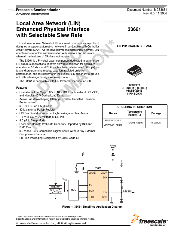
VPWR
33661 WAKE VDD
Regulator 12 V 5.0 V
VSUP INH
EN MCU RXD TXD LIN GND LIN Bus
Figure 1. 33661 Simplified Application Diagram
- This document contains certain information on a new product. Specifications and information herein are subject to change without notice.
© Freescale...