MCZ33689D
MCZ33689D is System Basis Chip manufactured by Freescale Semiconductor.
.. Freescale Semiconductor
Technical Data
Document Number: MC33689 Rev. 7.0, 8/2006
System Basis Chip with LIN Transceiver
The 33689 is a SPI-controlled System Basis Chip (SBC) that bines many frequently used functions in an MCU-based system plus a Local Interconnect Network (LIN) transceiver. Applications include power window, mirror, and seat controls. The 33689 has a 5.0 V, 50 m A low dropout regulator with full protection and reporting Features
. The device provide full SPI-readable diagnostics and a selectable timing watchdog for detecting errant operation. The LIN transceiver waveshaping circuitry can be disabled for higher data rates. One 50 m A and two 150 m A high-side switches with output protection are available to drive inductive or resistive loads. The 150 m A switches can be pulse-width modulated (PWM). Two high-voltage inputs are available for contact monitoring or as external wake-up inputs. A current sense operational amplifier is available for load current monitoring. The 33689 has three operational modes:
- Normal (all functions available)
- Sleep (VDD OFF, wake-up via LIN bus or wake-up inputs)
- Stop (VDD ON, wake-up via MCU, LIN bus, or wake-up inputs) Features
- -
- -
- -
- Full-Duplex SPI Interface at Frequencies up to 4.0 MHz LIN Transceiver Capable to 100 kbps with Waveshaping Capability 5.0 V Low Dropout Regulator Full Fault Detection and Protection One 50 m A and Two 150 m A Protected High-Side Switches Current Sense Operational Amplifier The 33689 is patible with LIN 2.0 Specification Package. Pb-Free Packaging Designated by Suffix Code EW
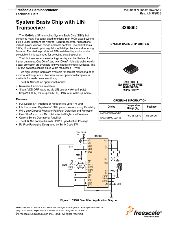
VDD VPWR
33689D
SYSTEM BASIS CHIP WITH LIN
DWB SUFFIX EW SUFFIX (PB-FREE) 98ARH99137A 32-PIN SOICW
ORDERING INFORMATION
Device MC33689DDWB/R2 MCZ33689DEW/R2 -40°C to 125°C 32 SOICW Temperature Range (TA) Package
VS1 VS2 VCC VDD WDC HS3 L1 L2
5.0 V
HS1 CS MCU SCK MOSI MISO SPI CS SCLK MOSI MISO INT RST IN OUT TXD RXD HS2 E+ EGND TGND AGND LIN
Figure 1. 33689...