Datasheet4U Logo Datasheet4U.com

MRF6S9160HR3 - RF Power Field Effect Transistors

Description

Ferrite Beads, Small 47 pF Chip Capacitors 0.8- 8.0 pF Variable Capacitors, Gigatrim 2.7 pF Chip Capacitor 15 pF Chip Capacitors 12 pF Chip Capacitors 4.3 pF Chip Capacitors 8.2 pF Chip Capacitor 3.9 pF Chip Capacitors 0.6- 4.5 pF Variable Capacitor, Gigatrim 22 pF Chip Capacitor 1 μF, 50 V Tantalum

Features

  • Characterized with Series Equivalent Large - Signal Impedance Parameters.
  • Internally Matched for Ease of Use.
  • Qualified Up to a Maximum of 32 VDD Operation.
  • Integrated ESD Protection.
  • Lower Thermal Resistance Package.
  • Low Gold Plating Thickness on Leads, 40μ″ Nominal.
  • RoHS Compliant.
  • In Tape and Reel. R3 Suffix = 250 Units per 56 mm, 13 inch Reel. MRF6S9160HR3 MRF6S9160HSR3 880 MHz, 35 W AVG. , 28 V SINGLE N - CDMA LATERA.

📥 Download Datasheet

Full PDF Text Transcription

Click to expand full text
www.DataSheet4U.com 
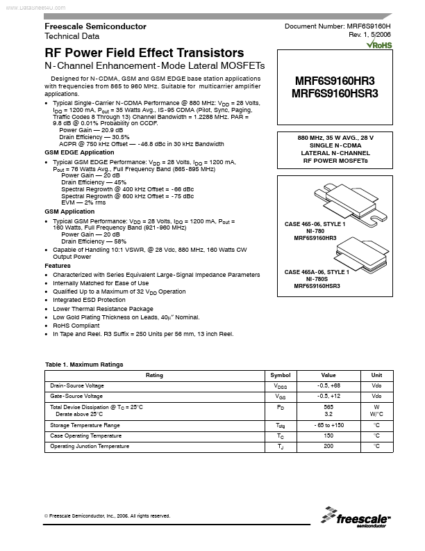
Freescale Semiconductor Technical Data Document Number: MRF6S9160H Rev. 1, 5/2006 RF Power Field Effect Transistors N - Channel Enhancement - Mode Lateral MOSFETs Designed for N - CDMA, GSM and GSM EDGE base station applications with frequencies from 865 to 960 MHz. Suitable for multicarrier amplifier applications. • Typical Single - Carrier N - CDMA Performance @ 880 MHz: VDD = 28 Volts, IDQ = 1200 mA, Pout = 35 Watts Avg., IS - 95 CDMA (Pilot, Sync, Paging, Traffic Codes 8 Through 13) Channel Bandwidth = 1.2288 MHz. PAR = 9.8 dB @ 0.01% Probability on CCDF. Power Gain — 20.9 dB Drain Efficiency — 30.5% ACPR @ 750 kHz Offset — - 46.8 dBc in 30 kHz Bandwidth GSM EDGE Application • Typical GSM EDGE Performance: VDD = 28 Volts, IDQ = 1200 mA, Pout = 76 Watts Avg.
Published: |