MB84VD2208xEA Key Features
- Power supply voltage of 2.7 to 3.3V
- High performance 90 ns maximum access time (Flash) 85 ns maximum access time (SRAM)
- Operating Temperature -25 to +85°C
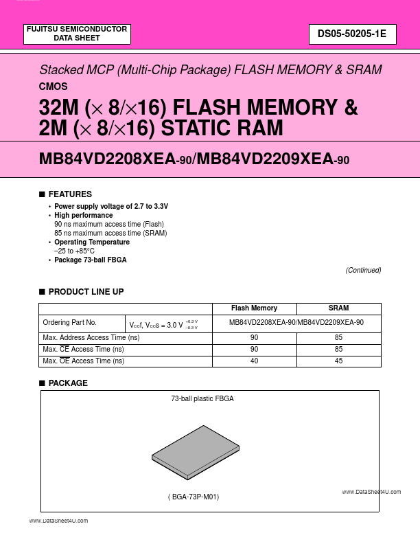
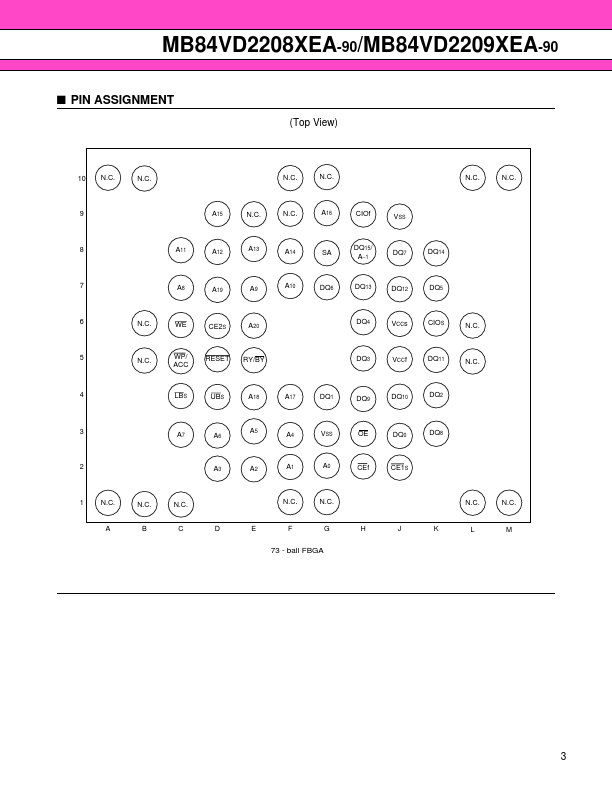
- Package 73-ball FBGA
- Simultaneous Read/Write operations (dual bank) Multiple devices available with different bank sizes Host system can prog
- Minimum 100,000 write/erase cycles
- Sector erase architecture Eight 4 K words and sixty three 32 K words. Any bination of sectors can be concurrently erased
- Boot Code Sector Architecture MB84VD2208XEA: Top sector MB84VD2209XEA: Bottom sector
- Embedded EraseTM Algorithms Automatically pre-programs and erases the chip or any sector
- Embedded ProgramTM Algorithms Automatically writes and verifies data at specified address