MB84VP23481FK-70 Description
FUJITSU SEMICONDUCTOR DATA SHEET DS05-50224-1E Stacked MCP (Multi-Chip Package) FLASH MEMORY & FCRAM CMOS 64M (×16) Page FLASH MEMORY & 32M (×16) Mobile FCRAMTM MB84VP23481FK-70.
MB84VP23481FK-70 Key Features
- Power Supply Voltage of 2.7 V to 3.1 V
- High Performance 25 ns maximum page read access time, 65 ns maximum random access time (Flash) 20 ns maximum page read a
- Operating Temperature -30 °C to +85 °C
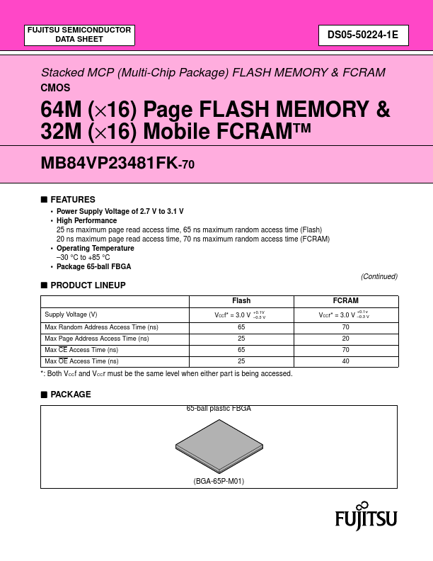
- Package 65-ball FBGA
- Both VCCf and VCCr must be the same level when either part is being accessed
- FLASH MEMORY
- Simultaneous Read/Write Operations (Dual Bank)
- 8 words Page
- patible with JEDEC-standard mands Uses same software mands as E2PROMs
- Minimum 100,000 Program/Erase Cycles