MBM29PL32TM Description
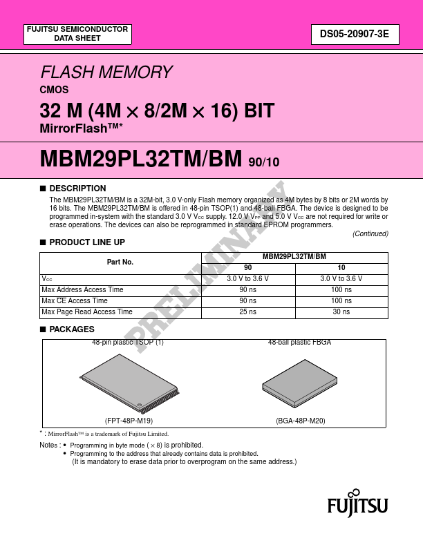
The MBM29PL32TM/BM is a 32M-bit, 3.0 V-only Flash memory organized as 4M bytes by 8 bits or 2M words by 16 bits. The MBM29PL32TM/BM is offered in 48-pin TSOP(1) and 48-ball FBGA. The device is designed to be programmed in-system with the standard 3.0 V VCC supply.