~D~~
FIELD EFFECT POWER TRANSISTOR
IRF150,151
D86FL2,K2
40 AMPERES
100,60 VOLTS
ROS(ON) = 0.055 il
This series of N:-Channel Enhancement-mode Power
MOSFETs utilizes GE's advanced Power DMOS technology
to achieve low on-resistance with excellent device rugged-
ness and reliability.
.
This design has been optimized to give superior performance
in most switching applications including: switching power
supplies, inverters, converters and solenoid/relay drivers.
Also, the extended safe operating area with good linear
transfer characteristics makes it well suited for many linear
applications such as audio amplifiers and servo motors.
Features
• Polysilicon gate - Improved stability and reliability
• No secondary breakdown - Excellent ruggedness
• Ultra-fast switching - Independent of temperature
• Voltage controlled - High transconductance
• Low input capacitance - Reduced drive requirement
• Excellent thermal stability - Ease of paralleling
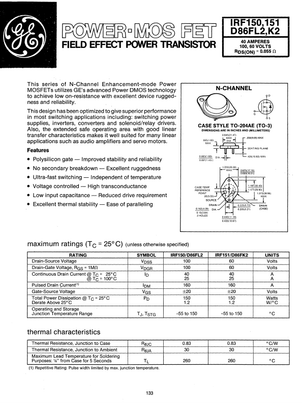
N-CHANNEL
CASE STYLE TO-204AE (TO-3)
DIMENSIONS ARE IN INCHES AND (MILLIMETERS)
0845(21.47)
",;~r:."~~ ,~,~~-MAX.H·35819.09J MAX
0.063(1.60) DIA......J L
0.057(1.45)
II
.426(10.82) MIN.
CASE TEMP.
REFERENCE
POINT
.20(5.00)
0.162(4.09)
0.15(3.84)
2 HOLES
DIA.
0.440(11.18)
0.420110.67)
=maximum ratings (TC 250 C) (unless otherwise specified)
RATING
Drain-Source Voltage
Drain-Gate Voltage, RGS = 1Mil
Continuous Drain Current @ TC = 25° C
@TC= 100°C
Pulsed Drain 9urrent(1)
Gate-Source Voltage
Total Power Dissipation @TC = 25°C
Derate Above 25° C
Operating and Storage
Junction Temperature Range
SYMBOL
Voss
VOGR
10
10M
VGS
Po
TJ, TSTG
IRF150/086FL2
100
100
40
25
160
±20
150
1.2
-55 to 150
IRF151/086FK2
60
60
40
25
160
±20
150
1.2
-55 to 150
thermal characteristics
Thermal Resistance, Junction to Case
R8JC
Thermal Resistance, Junction to Ambient
R8JA
Maximum Lead Temperature for Soldering
Purposes: Va" from Case for 5 Seconds
TL
(1) Repetitive Rating: Pulse width limited by max. junction temperature.
0.83
30
260
0.83
30
260
UNITS
Volts
Volts
A
A
A
Volts
Watts
WloC
°C
°CIW
°CIW
°C
133