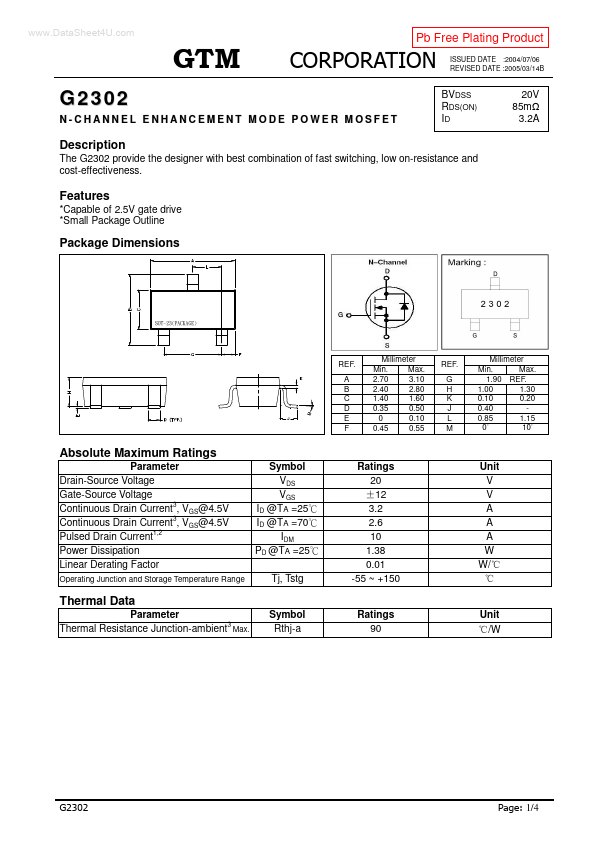
G2302 Description
Capable of 2.5V gate drive Small Package Outline.
G2302 is N-CHANNEL ENHANCEMENT MODE POWER MOSFET manufactured by GTM.
| Part Number | Description |
|---|---|
| G2300 | CMOS Positive Voltage Regulator |
| G2301 | P-CHANNEL ENHANCEMENT MODE POWER MOSFET |
| G2303 | P-CHANNEL ENHANCEMENT MODE POWER MOSFET |
| G2304 | N-CHANNEL ENHANCEMENT MODE POWER MOSFET |
| G2304A | N-CHANNEL ENHANCEMENT MODE POWER MOSFET |
Capable of 2.5V gate drive Small Package Outline.