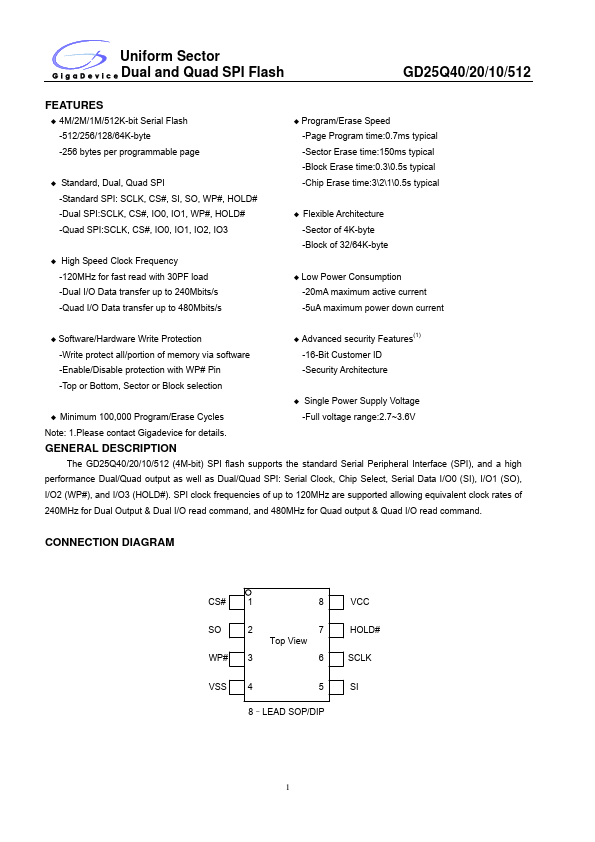
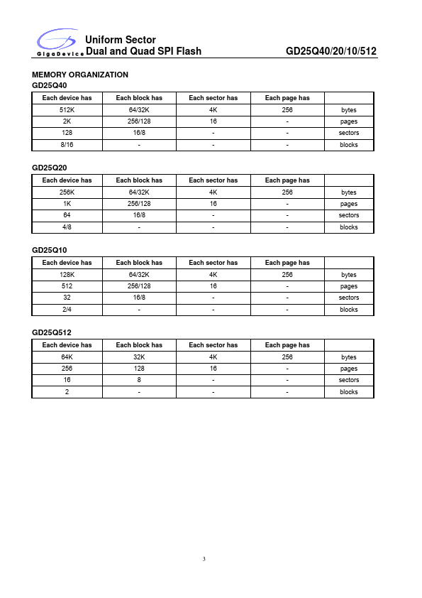
GD25Q10 Description
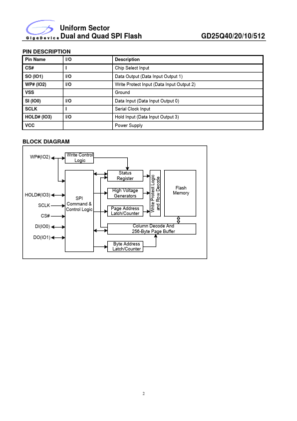
The GD25Q40/20/10/512 (4M-bit) SPI flash supports the standard Serial Peripheral Interface (SPI), and a high performance Dual/Quad output as well as Dual/Quad SPI: Serial Clock, Chip Select, Serial Data I/O0 (SI), I/O1 (SO), I/O2 (WP#), and I/O3 (HOLD#). SPI clock frequencies of up to 120MHz are supported allowing equivalent clock rates of 240MHz for Dual Output & Dual I/O read mand, and 480MHz for Quad output &...
GD25Q10 Key Features
- 4M/2M/1M/512K-bit Serial Flash -512/256/128/64K-byte -256 bytes per programmable page
- Standard, Dual, Quad SPI -Standard SPI: SCLK, CS#, SI, SO, WP#, HOLD# -Dual SPI:SCLK, CS#, IO0, IO1, WP#, HOLD# -Quad SP
- High Speed Clock Frequency -120MHz for fast read with 30PF load -Dual I/O Data transfer up to 240Mbits/s -Quad I/O Data
- Program/Erase Speed -Page Program time:0.7ms typical -Sector Erase time:150ms typical -Block Erase time:0.3�.5s typical
- Flexible Architecture -Sector of 4K-byte -Block of 32/64K-byte
- Low Power Consumption -20mA maximum active current -5uA maximum power down current
- Software/Hardware Write Protection
- Advanced security Features(1)
- Write protect all/portion of memory via software
- 16-Bit Customer ID