Datasheet4U Logo Datasheet4U.com

HMS1M32Z8 - SRAM MODULE 4Mbyte

Download the HMS1M32Z8 datasheet PDF. This datasheet also covers the HMS1M32M8G variant, as both devices belong to the same sram module 4mbyte family and are provided as variant models within a single manufacturer datasheet.

General Description

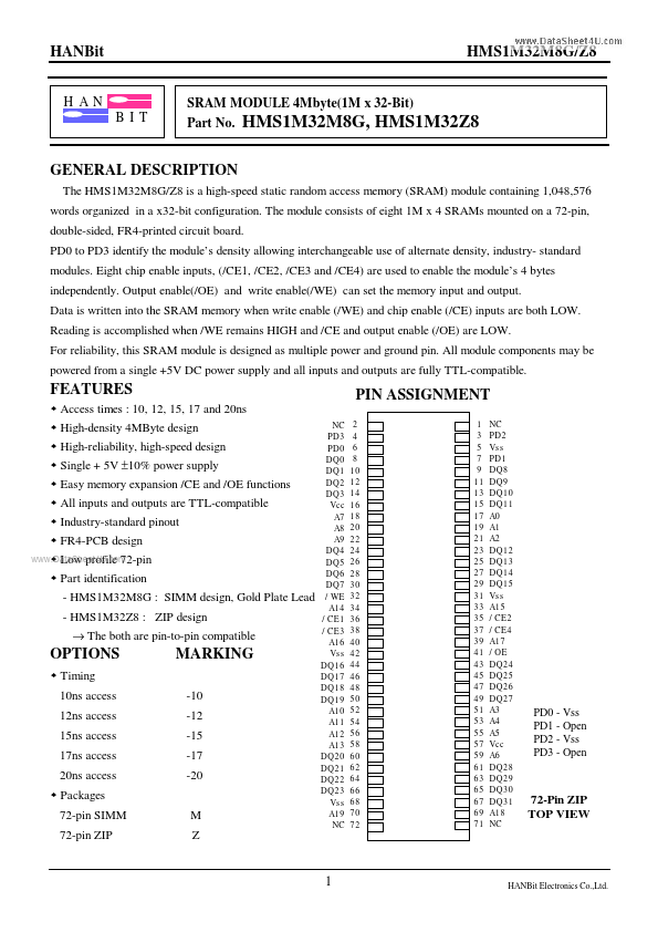
The HMS1M32M8G/Z8 is a high-speed static random access memory (SRAM) module containing 1,048,576 words organized in a x32-bit configuration.

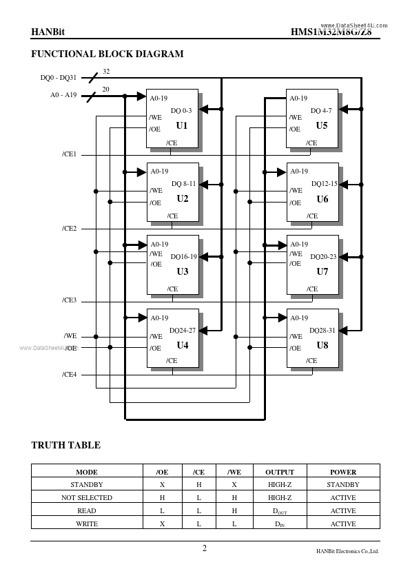
The module consists of eight 1M x 4 SRAMs mounted on a 72-pin, double-sided, FR4-printed circuit board.

Key Features

  • Access times : 10, 12, 15, 17 and 20ns.
  • High-density 4MByte design.
  • High-reliability, high-speed design.
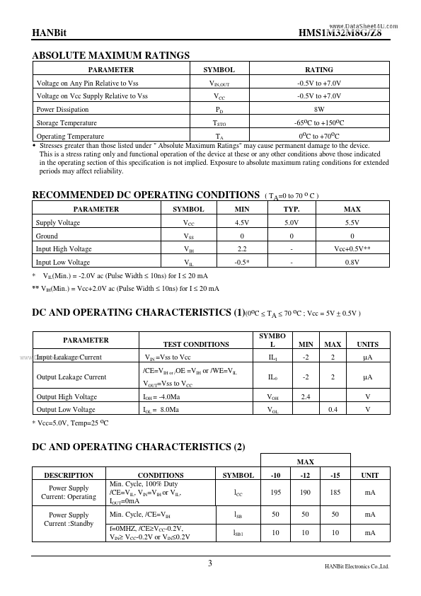
  • Single + 5V ±10% power supply.
  • Easy memory expansion /CE and /OE functions.
  • All inputs and outputs are TTL-compatible.
  • Industry-standard pinout.
  • FR4-PCB design www. DataSheet4U. com.
  • Low profile 72-pin.
  • Part identification - HMS1M32M8G : SIMM design, Gold Plate Lead - HMS1M32Z8 : ZIP design → The both are pin-to-pin compatible NC PD3 PD0 DQ0 DQ.

📥 Download Datasheet

Note: The manufacturer provides a single datasheet file (HMS1M32M8G_HanbitElectronics.pdf) that lists specifications for multiple related part numbers.

Datasheet Details

Part number HMS1M32Z8
Manufacturer Hanbit Electronics
File Size 104.54 KB
Description SRAM MODULE 4Mbyte
Datasheet download datasheet HMS1M32Z8 Datasheet

Full PDF Text Transcription (Reference)

The following content is an automatically extracted verbatim text from the original manufacturer datasheet and is provided for reference purposes only.

View original datasheet text
HANBit HAN BIT HMS1M32M8G/Z8 SRAM MODULE 4Mbyte(1M x 32-Bit) Part No. HMS1M32M8G, HMS1M32Z8 GENERAL DESCRIPTION The HMS1M32M8G/Z8 is a high-speed static random access memory (SRAM) module containing 1,048,576 words organized in a x32-bit configuration. The module consists of eight 1M x 4 SRAMs mounted on a 72-pin, double-sided, FR4-printed circuit board. PD0 to PD3 identify the module’s density allowing interchangeable use of alternate density, industry- standard modules. Eight chip enable inputs, (/CE1, /CE2, /CE3 and /CE4) are used to enable the module’s 4 bytes independently. Output enable(/OE) and write enable(/WE) can set the memory input and output. Data is written into the SRAM memory when write enable (/WE) and chip enable (/CE) inputs are both LOW.