MSA-1110
MSA-1110 is Cascadable Silicon Bipolar MMIC Amplifier manufactured by Hewlett-Packard.
- Part of the MSA-1110_Hewlett comparator family.
- Part of the MSA-1110_Hewlett comparator family.
Features
- High Dynamic Range Cascadable 50 Ω or 75 Ω Gain Block
- 3 d B Bandwidth: 50 MHz to 1.6 GHz
- 17.5 d Bm Typical P1 d B at 0.5 GHz
- 12 d B Typical 50 Ω Gain at 0.5 GHz
- 3.5 d B Typical Noise Figure at 0.5 GHz
- Hermetic Gold-ceramic Microstrip Package
Description
The MSA-1110 is a high performance silicon bipolar Monolithic Microwave Integrated Circuit (MMIC) housed in a hermetic high reliability package. This MMIC is designed for high dynamic range in either 50 or 75 Ω systems by bining low noise figure with high IP3. Typical applications include narrow and broadband linear amplifiers in industrial and military systems. The MSA-series is fabricated using Agilent’s 10 GHz f T, 25 GHz f MAX silicon bipolar MMIC process which uses nitride self-alignment, ion implantation, and gold metallization to achieve excellent performance, uniformity and reliability. The use of an external bias resistor for temperature and current stability also allows bias flexibility.
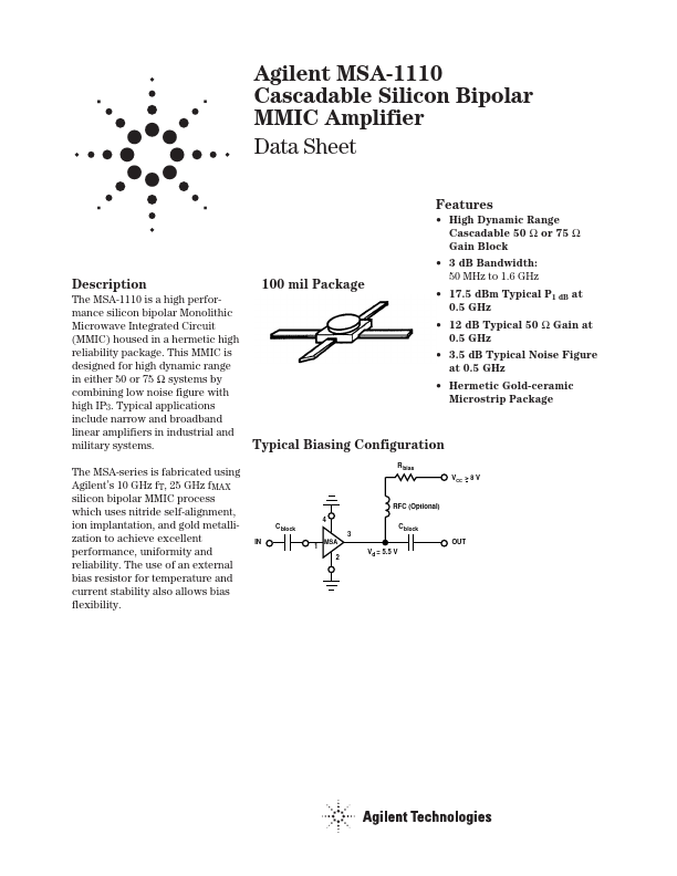
100 mil Package
Typical Biasing Configuration
R bias VCC > 8 V
RFC (Optional) 4 C block 3 IN 1
C block OUT Vd = 5.5 V
MSA-1110 Absolute Maximum Ratings
Parameter Device Current Power Dissipation[2,3] RF Input Power Junction Temperature Storage Temperature Absolute Maximum[1] 90 m A 560 m W +13 d Bm 200°C
- 65 to 200°C Thermal Resistance[2, 4]: θjc = 135°C/W
Notes: 1. Permanent damage may occur if any of these limits are exceeded. 2. TCASE = 25°C. 3. Derate at 7.4 m W/°C for TC > 124°C. 4. The small spot size of this technique results in a higher, though more accurate determination of θjc than do alternate methods.
Electrical Specifications[1], TA = 25°C
Symbol
GP ∆G P f3 d B VSWR NF P1 d B IP3 t D Vd d V/d T
Parameters and Test Conditions: Id = 60 m A, ZO = 50 Ω
Power Gain (|S21| 2) Gain Flatness 3 d B Bandwidth[2] Input VSWR Output VSWR 50 Ω Noise Figure Output Power at 1 d B Gain pression Third Order Intercept Point Group Delay Device Voltage Device Voltage Temperature Coefficient f = 0.1 to 1.0 GHz f...