BB101M
Features
- Build in Biasing Circuit; To reduce using parts cost & PC board space.
- Low noise characteristics; (NF = 2.0 d B typ. at f = 900 MHz)
- Withstanding to ESD; Build in ESD absorbing diode. Withstand up to 200 V at C = 200 p F, Rs = 0 conditions.
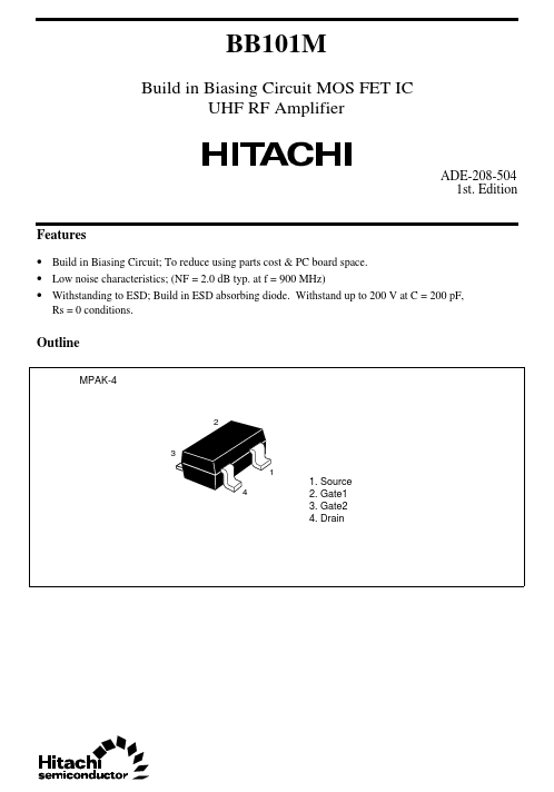
Outline
MPAK-4
3 1 4
1. Source 2. Gate1 3. Gate2 4. Drain
Absolute Maximum Ratings (Ta = 25°C)
Item Drain to source voltage Gate 1 to source voltage Gate 2 to source voltage Drain current Channel power dissipation Channel temperature Storage temperature Symbol VDS VG1S VG2S ID Pch Tch Tstg Ratings 6 +6
- 0 ±6 25 150 150
- 55 to +150 Unit V V V m A m W °C °C
Electrical Characteristics (Ta = 25°C)
Item Drain to source breakdown voltage Gate 1 to source breakdown voltage Gate 2 to source breakdown voltage Symbol V(BR)DSS V(BR)G1SS V(BR)G2SS Min 6 +6 ±6
- - 0.2 0.4 10 16 Typ
- -
- -
- -
- 15 22 Max
- -
- +100 ±100 0.8 1.0 20
- Unit V V V n A n A V V m A m S Test conditions I D = 200 µA VG1S = VG2S = 0 I G1 = +10 µA VG2S =...