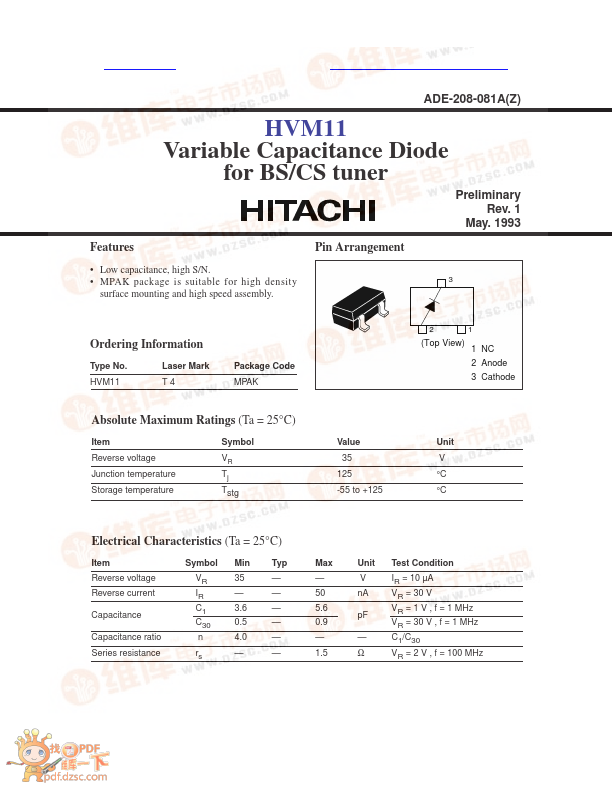
Datasheet4U Logo Datasheet4U.com

HVM11 - Variable Capacitance Diode

Key Features

  • Pin Arrangement.
  • Low capacitance, high S/N.
  • MPAK package is suitable for high density surface mounting and high speed assembly. 3 Ordering Information Type No. HVM11 Laser Mark T4 Package Code MPAK 21 (Top View) 1 NC 2 Anode 3 Cathode Absolute Maximum Ratings (Ta = 25°C) Item Reverse voltage Junction temperature Storage temperature Symbol VR Tj Tstg Value 35 125 -55 to +125 Unit V °C °C Electrical Characteristics (Ta = 25°C) Item Reverse voltage Reverse current.

📥 Download Datasheet

Full PDF Text Transcription (Reference)

The following content is an automatically extracted verbatim text from the original manufacturer datasheet and is provided for reference purposes only.

View original datasheet text
ADE-208-081A(Z) HVM11 Variable Capacitance Diode for BS/CS tuner Preliminary Rev. 1 May. 1993 Features Pin Arrangement • Low capacitance, high S/N. • MPAK package is suitable for high density surface mounting and high speed assembly. 3 Ordering Information Type No. HVM11 Laser Mark T4 Package Code MPAK 21 (Top View) 1 NC 2 Anode 3 Cathode Absolute Maximum Ratings (Ta = 25°C) Item Reverse voltage Junction temperature Storage temperature Symbol VR Tj Tstg Value 35 125 -55 to +125 Unit V °C °C Electrical Characteristics (Ta = 25°C) Item Reverse voltage Reverse current Capacitance Capacitance ratio Series resistance Symbol VR IR C1 C30 n rs Min 35 — 3.6 0.5 4.0 — Typ — — — — — — Max Unit Test Condition — V IR = 10 µA 50 nA VR = 30 V 5.6 pF VR = 1 V , f = 1 MHz 0.