2SK2216 Overview
Key Specifications
Key Features
- High power output, high gain, high efficiency PG = 9.7 dB, Pout = 140 W, ηD = 55% typ (f = 860 MHz)
- Compact package Suitable for push
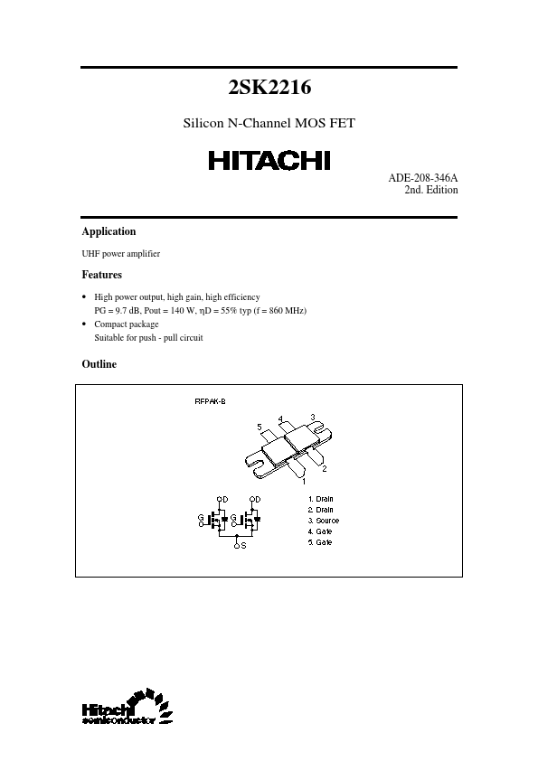
- pull circuit Outline 2SK2216
| Part | 2SK2216 |
|---|---|
| Description | Silicon N-Channel MOS FET |
| Manufacturer | Hitachi Semiconductor |
| Size | 47.53 KB |
| Seller | Inventory | Price Breaks | Buy |
|---|---|---|---|
| No distributor offers were returned for this part. | |||
| Part Number | Manufacturer | Description |
|---|---|---|
| 2SK2213-01L | Fuji Electric | N-channel MOS-FET |
| 2SK2215-01S | Fuji Electric | N-channel MOS-FET |
| 2SK2211 | Kexin Semiconductor | N-Channel MOSFET |
| 2SK2215-01L | Fuji Electric | N-channel MOS-FET |
| 2SK2211 | VBsemi | 30V N-Channel MOSFET |