HD74HC534
Overview
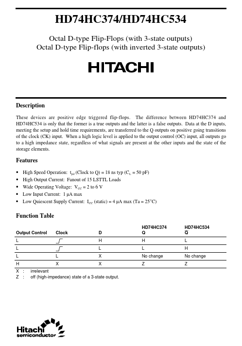
These devices are positive edge triggered flip-flops. The difference between HD74HC374 and HD74HC534 is only that the former is a true outputs and the latter is a false outputs.
- High Speed Operation: tpd (Clock to Q) = 18 ns typ (CL = 50 pF) High Output Current: Fanout of 15 LSTTL Loads Wide Operating Voltage: VCC = 2 to 6 V Low Input Current: 1 µA max Low Quiescent Supply Current: ICC (static) = 4 µA max (Ta = 25°C)