Click to expand full text
HY5DU281622ET
128M(8Mx16) GDDR SDRAM
HY5DU281622ET
This document is a general product description and is subject to change without notice. Hynix Electronics does not assume any responsibility for use of circuits described. No patent licenses are implied. Rev. 0.5 / Jan. 2005 1
HY5DU281622ET
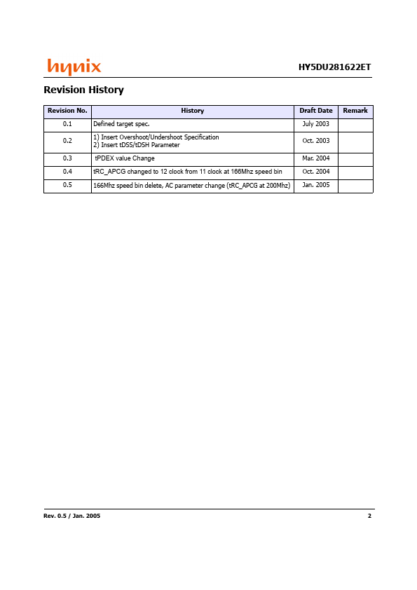
Revision History
Revision No. 0.1 0.2 0.3 0.4 0.5 Defined target spec. 1) Insert Overshoot/Undershoot Specification 2) Insert tDSS/tDSH Parameter tPDEX value Change tRC_APCG changed to 12 clock from 11 clock at 166Mhz speed bin 166Mhz speed bin delete, AC parameter change (tRC_APCG at 200Mhz) History Draft Date July 2003 Oct. 2003 Mar. 2004 Oct. 2004 Jan. 2005 Remark
Rev. 0.5 / Jan.
 HY5DU281622ET Datasheet