Datasheet4U Logo Datasheet4U.com

HY5S2B6DLFP-SE - 4Banks x 2M x 16bits Synchronous DRAM

Download the HY5S2B6DLFP-SE datasheet PDF. This datasheet also covers the HY5S2B6DLF-BE variant, as both devices belong to the same 4banks x 2m x 16bits synchronous dram family and are provided as variant models within a single manufacturer datasheet.

📥 Download Datasheet

Note: The manufacturer provides a single datasheet file (HY5S2B6DLF-BE_HynixSemiconductor.pdf) that lists specifications for multiple related part numbers.

General Description

and is subject to change without notice.

Hynix Semiconductor does not assume any responsibility for use of circuits described.

No patent licenses are implied.
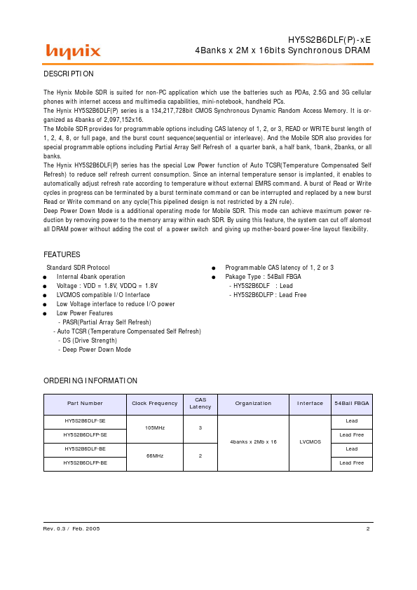
Overview

HY5S2B6DLF(P)-xE 4Banks x 2M x 16bits Synchronous DRAM Document Title 4Bank x 2M x 16bits Synchronous DRAM Revision History Revision No.

0.1 0.2 0.3 History Initial Draft Deleted Preliminary Changed Operation Voltage : 1.65(min) -> 1.70(min) Draft Date Dec.

2003 May.

Key Features

  • Standard SDR Protocol Internal 4bank operation.
  • Voltage : VDD = 1.8V, VDDQ = 1.8V.
  • LVCMOS compatible I/O Interface.
  • Low Voltage interface to reduce I/O power.
  • Low Power Features - PASR(Partial Array Self Refresh) - Auto TCSR (Temperature Compensated Self Refresh) - DS (Drive Strength) - Deep Power Down Mode.
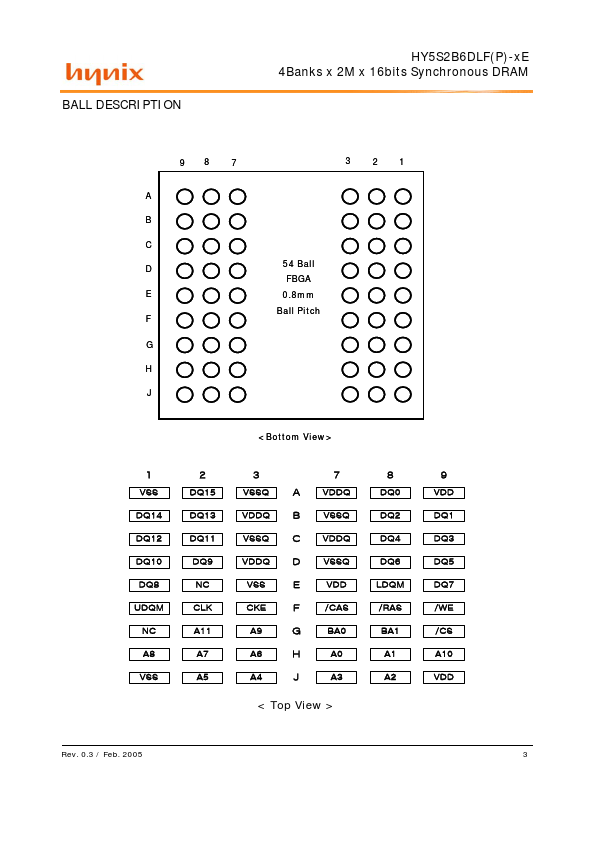
  • Programmable CAS latency of 1, 2 or 3 Pakage Type : 54Ball FBGA - HY5S2B6DLF : Lead - HY5S2B6DLFP : Lead Free.