1.8V to 3.3V LVCMOS High-Performance
Clock Buffer Family
5PB11xx
DATASHEET
Description
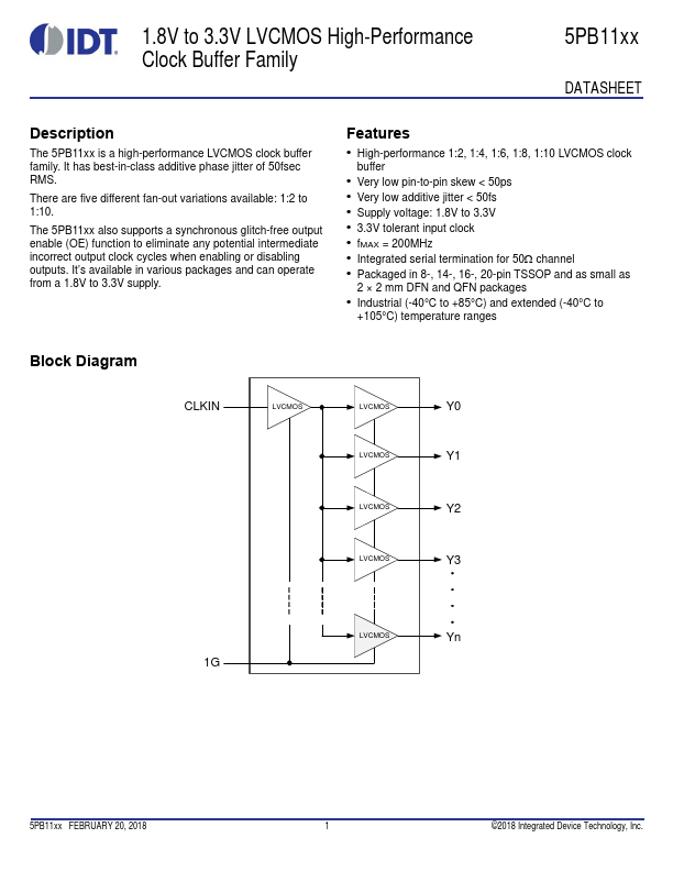
The 5PB11xx is a high-performance LVCMOS clock buffer
family. It has best-in-class additive phase jitter of 50fsec
RMS.
There are five different fan-out variations available: 1:2 to
1:10.
The 5PB11xx also supports a synchronous glitch-free output
enable (OE) function to eliminate any potential intermediate
incorrect output clock cycles when enabling or disabling
outputs. It’s available in various packages and can operate
from a 1.8V to 3.3V supply.
Features
• High-performance 1:2, 1:4, 1:6, 1:8, 1:10 LVCMOS clock
buffer
• Very low pin-to-pin skew < 50ps
• Very low additive jitter < 50fs
• Supply voltage: 1.8V to 3.3V
• 3.3V tolerant input clock
• fMAX = 200MHz
• Integrated serial termination for 50 channel
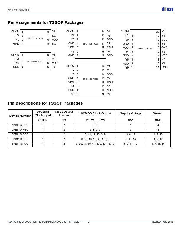
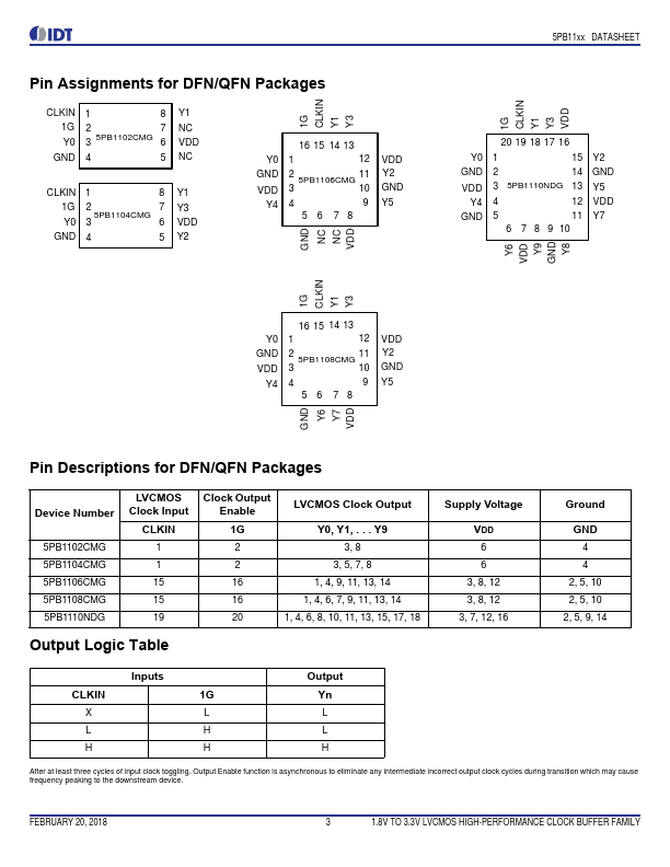
• Packaged in 8-, 14-, 16-, 20-pin TSSOP and as small as
2 × 2 mm DFN and QFN packages
• Industrial (-40°C to +85°C) and extended (-40°C to
+105°C) temperature ranges
Block Diagram
CLKIN
LVCMOS
LVCMOS
Y0
LVCMOS
Y1
LVCMOS
Y2
LVCMOS
Y3
LVCMOS
Yn
1G
5PB11xx FEBRUARY 20, 2018
1 ©2018 Integrated Device Technology, Inc.