ICS854S006I
ICS854S006I is Differential-to-LVDS Fanout Buffer manufactured by IDT.
Low Skew, 1-to-6, Differential-to LVDS Fanout Buffer
DATA SHEET
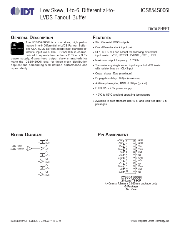
GENERAL DESCRIPTION
The ICS854S006I is a low skew, high perfor ICS mance 1-to-6 Differential-to-LVDS Fanout Buffer. Hi Per Clock S™ The CLK, n CLK pair can accept most standard dif- ferential input levels. The ICS854S006I is characterized to operate from either a 2.5V or a 3.3V power supply. Guaranteed output skew characteristic s make the ICS854S006I ideal for those clock distribution applications demanding well defined performance and r e p e a t a b i l i t y.
Features
- Six differential LVDS outputs
- One differential clock input pair
- CLK, n CLK pair can accept the following differential input levels: LVDS, LVPECL, LVHSTL, SSTL, HCSL
- Maximum output frequency: 1.7GHz
- Translates any single ended input signal to LVDS levels with resistor bias on n CLK input
- Output skew: 55ps (maximum)
- Propagation delay: 850ps (maximum)
- Additive phase jitter, RMS: 0.067ps (typical)
- Full 3.3V or...