IDT71V35781SA
IDT71V35781SA is 3.3V Synchronous SRAMs manufactured by IDT.
- Part of the IDT71V35761S comparator family.
- Part of the IDT71V35761S comparator family.
128K x 36, 256K x 18 3.3V Synchronous SRAMs 3.3V I/O, Pipelined Outputs Burst Counter, Single Cycle Deselect
IDT71V35761S IDT71V35781S IDT71V35761SA IDT71V35781SA
Features x 128K x 36, 256K x 18 memory configurations x Supports high system speed: mercial:
- 200MHz 3.1ns clock access time mercial and Industrial:
- 183MHz 3.3ns clock access time
- 166MHz 3.5ns clock access time x LBO input selects interleaved or linear burst mode x Self-timed write cycle with global write control (GW), byte write enable (BWE), and byte writes (BWx) x 3.3V core power supply x Power down controlled by ZZ input x 3.3V I/O x Optional
- Boundary Scan JTAG Interface (IEEE 1149.1 pliant) x Packaged in a JEDEC Standard 100-pin plastic thin quad flatpack (TQFP), 119 ball grid array (BGA) and 165 fine pitch ball grid array
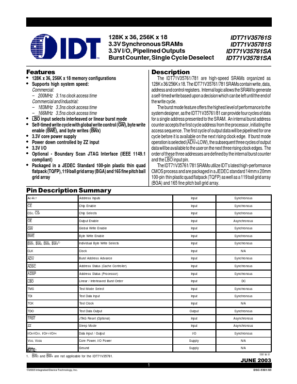
Pin Description Summary
Description
The IDT71V35761/781 are high-speed SRAMs organized as 128K x 36/256K x 18. The IDT71V35761/781 SRAMs contain write, data, addressandcontrolr...