2N3864 Overview
Description
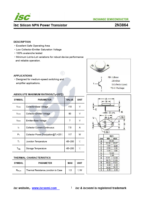
Excellent Safe Operating Area - Low Collector-Emitter Saturation Voltage - 100% avalanche tested - Minimum Lot-to-Lot variations for robust device performance and reliable operation.
| Part | 2N3864 |
|---|---|
| Description | NPN Transistor |
| Category | Transistor |
| Manufacturer | Inchange Semiconductor |
| Size | 178.57 KB |
Excellent Safe Operating Area - Low Collector-Emitter Saturation Voltage - 100% avalanche tested - Minimum Lot-to-Lot variations for robust device performance and reliable operation.
| Part Number | Manufacturer | Description |
|---|---|---|
| 2N3867 | Microsemi | Silicon PNP Power Transistors |
| 2N3866 | NXP Semiconductors | Silicon planar epitaxial overlay transistors |
| 2N3866 | Microsemi | RF & MICROWAVE DISCRETE LOW-POWER TRANSISTORS |
| 2N3866 | Motorola Semiconductor | HIGH-FREQUENCY TRANSISTOR |
| 2N3866A | Central Semiconductor | NPN SILICON HIGH FREQUENCY TRANSISTOR |