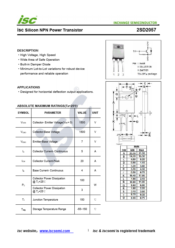
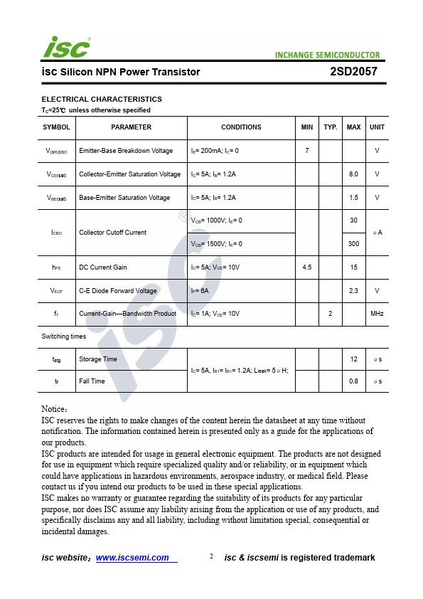
The following content is an automatically extracted verbatim text
from the original manufacturer datasheet and is provided for reference purposes only.
View original datasheet text
isc Silicon NPN Power Transistor
DESCRIPTION ·High Voltage, High Speed ·Wide Area of Safe Operation ·Built-in Damper Diode ·Minimum Lot-to-Lot variations for robust device
performance and reliable operation
APPLICATIONS ·Designed for horizontal deflection output applications.
ABSOLUTE MAXIMUM RATINGS(Ta=25℃)
SYMBOL
PARAMETER
VALUE
UNIT
VCES
Collector- Emitter Voltage(VBE= 0)
1500
V
VCBO
Collector-Base Voltage
1500
V
VEBO
Emitter-Base Voltage
7
V
IC
Collector Current- Continuous
5
A
ICM
Collector Current-Peak
20
A
IB
Base Current- Continuous
Collector Power Dissipation @ TC=25℃ PC Collector Power Dissipation @ Ta=25℃
TJ
Junction Temperature
4
A
100 W
3
150
℃
Tstg
Storage Temperature Range
-55~150
℃
2SD2057
isc website:www.iscsemi.