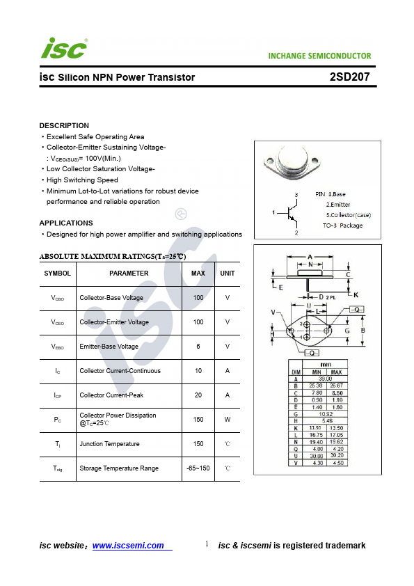
Excellent Safe Operating Area
Collector-Emitter Sustaining Voltage-
: VCEO(SUS)= 100V(Min.)
Low Collector Saturation Voltage
High Switching Speed
Minimum Lot-to-Lot variations for robust device
performance and reliable operation
APPLICATIONS
Designed for high power ampl
The following content is an automatically extracted verbatim text
from the original manufacturer datasheet and is provided for reference purposes only.
View original datasheet text
isc Silicon NPN Power Transistor
INCHANGE Semiconductor
2SD207
DESCRIPTION ·Excellent Safe Operating Area ·Collector-Emitter Sustaining Voltage-
: VCEO(SUS)= 100V(Min.) ·Low Collector Saturation Voltage·High Switching Speed ·Minimum Lot-to-Lot variations for robust device
performance and reliable operation
APPLICATIONS ·Designed for high power amplifier and switching applications
ABSOLUTE MAXIMUM RATINGS(Ta=25℃)
SYMBOL
PARAMETER
MAX
UNIT
VCBO
Collector-Base Voltage
100
V
VCEO
Collector-Emitter Voltage
100
V
VEBO
Emitter-Base Voltage
6
V
IC
Collector Current-Continuous
10
A
ICP
Collector Current-Peak
PC
Collector Power Dissipation @TC=25℃
Tj
Junction Temperature
20
A
150
W
150
℃
Tstg
Storage Temperature Range
-65~150 ℃
isc website:www.iscsemi.