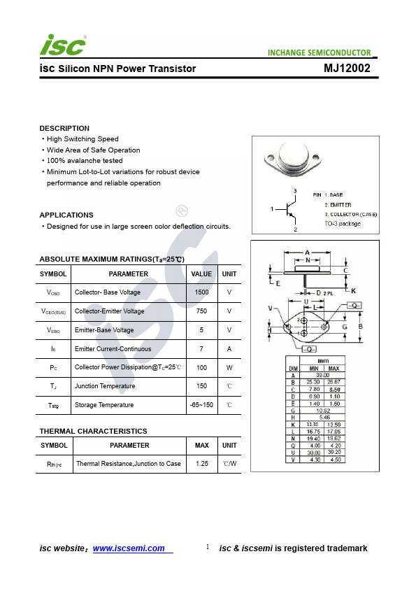
The following content is an automatically extracted verbatim text
from the original manufacturer datasheet and is provided for reference purposes only.
View original datasheet text
isc Silicon NPN Power Transistor
DESCRIPTION ·High Switching Speed ·Wide Area of Safe Operation ·100% avalanche tested ·Minimum Lot-to-Lot variations for robust device
performance and reliable operation
APPLICATIONS ·Designed for use in large screen color deflection circuits.
ABSOLUTE MAXIMUM RATINGS(Ta=25℃)
SYMBOL
PARAMETER
VALUE
UNIT
VCBO Collector- Base Voltage
1500
V
VCEO(SUS) Collector-Emitter Voltage
750
V
VEBO
Emitter-Base Voltage
5
V
IE
Emitter Current-Continuous
7
A
PC
Collector Power Dissipation@TC=25℃ 100
W
TJ
Junction Temperature
150
℃
Tstg
Storage Temperature
-65~150 ℃
THERMAL CHARACTERISTICS
SYMBOL
PARAMETER
Rth j-c Thermal Resistance,Junction to Case
MAX 1.25
UNIT ℃/W
MJ12002
isc website:www.iscsemi.