Datasheet4U Logo Datasheet4U.com

IS64WV25616LEBLL - 256K x 16 HIGH SPEED ASYNCHRONOUS CMOS STATIC RAM

Download the IS64WV25616LEBLL datasheet PDF. This datasheet also covers the IS61WV25616LEBLL variant, as both devices belong to the same 256k x 16 high speed asynchronous cmos static ram family and are provided as variant models within a single manufacturer datasheet.

General Description

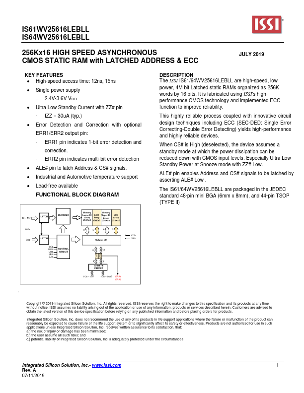
The ISSI IS61/64WV25616LEBLL are high-speed, low power, 4M bit Latched static RAMs organized as 256K words by 16 bits.

It is fabricated using ISSI's highperformance CMOS technology and implemented ECC function to improve reliability.

Key Features

  • High-speed access time: 12ns, 15ns.
  • Single power supply.
  • 2.4V-3.6V VDD.
  • Ultra Low Standby Current with ZZ# pin - IZZ = 30uA (typ. ).
  • Error Detection and Correction with optional ERR1/ERR2 output pin: - ERR1 pin indicates 1-bit error detection and correction. - ERR2 pin indicates multi-bit error detection.
  • ALE# pin to latch Address & CS# signals.
  • Industrial and Automotive temperature support.
  • Lead-free available.

📥 Download Datasheet

Note: The manufacturer provides a single datasheet file (IS61WV25616LEBLL-ISSI.pdf) that lists specifications for multiple related part numbers.

Full PDF Text Transcription (Reference)

The following content is an automatically extracted verbatim text from the original manufacturer datasheet and is provided for reference purposes only.

View original datasheet text
IS61WV25616LEBLL IS64WV25616LEBLL 256Kx16 HIGH SPEED ASYNCHRONOUS CMOS STATIC RAM with LATCHED ADDRESS & ECC JULY 2019 KEY FEATURES  High-speed access time: 12ns, 15ns  Single power supply – 2.4V-3.6V VDD  Ultra Low Standby Current with ZZ# pin - IZZ = 30uA (typ.)  Error Detection and Correction with optional ERR1/ERR2 output pin: - ERR1 pin indicates 1-bit error detection and correction. - ERR2 pin indicates multi-bit error detection  ALE# pin to latch Address & CS# signals.  Industrial and Automotive temperature support  Lead-free available FUNCTIONAL BLOCK DIAGRAM A0 – A17 LATCH DECODER ALE# CS# LATCH OE# WE# UB# LB# ZZ# CONTROL CIRCUIT .