BSR202N
BSR202N is Small Signal Transistor manufactured by Infineon.
..
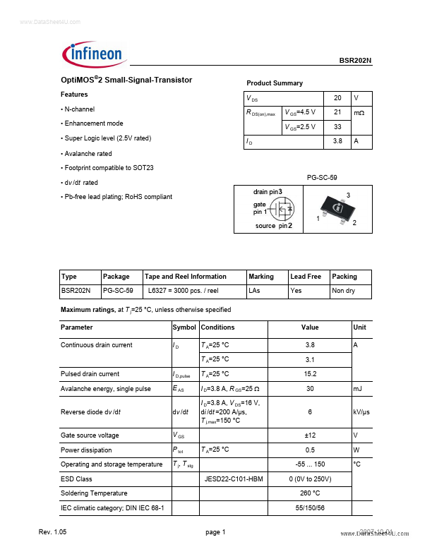
Opti MOS®2 Small-Signal-Transistor
Features
- N-channel
- Enhancement mode
- Super Logic level (2.5V rated)
- Avalanche rated
- Footprint patible to SOT23
- dv /dt rated
- Pb-free lead plating; Ro HS pliant
Product Summary V DS R DS(on),max V GS=4.5 V V GS=2.5 V ID 20 21 33 3.8 A V mΩ
PG-SC-59 3 1
Type BSR202N
Package PG-SC-59
Tape and Reel Information L6327 = 3000 pcs. / reel
Marking LAs
Lead Free Yes
Packing Non dry
Maximum ratings, at T j=25 °C, unless otherwise specified Parameter Continuous drain current Symbol Conditions ID T A=25 °C T A=25 °C Pulsed drain current Avalanche energy, single pulse Reverse diode d v /dt Gate source voltage Power dissipation Operating and storage temperature ESD Class Soldering Temperature IEC climatic category; DIN IEC 68-1 I D,pulse E AS dv /dt V GS P tot T j, T stg JESD22-C101-HBM T A=25 °C T A=25 °C I D=3.8 A, R GS=25 Ω I D=3.8 A, V DS=16 V, di /dt =200 A/µs, T j,max=150 °C Value 3.8 3.1 15.2 30 6 ±12 0.5 -55 ... 150 0 (0V to 250V) 260 °C 55/150/56 m J k V/µs V W °C Unit A
Rev. 1.05 page 1
2007-10-01
..
Parameter Symbol Conditions min. Thermal characteristics Thermal resistance, junction
- minimal footprint R th JA Values typ. max. Unit
- -
K/W
Electrical characteristics, at T j=25 °C, unless otherwise specified Static characteristics V (BR)DSS V GS= 0 V, I D= 250 µA V GS(th) I DSS V DS=0 V, I D=30 µA V DS=20 V, V GS=0 V, T j=25 °C V DS=20 V, V GS=0 V, T j=150 °C Gate-source leakage current Drain-source on-state resistance I GSS R DS(on) V GS=12 V, V DS=0 V V GS=2.5 V, I D=3 A V GS=4.5 V, I D=3.8 A Transconductance g fs |V DS|>2|I D|R DS(on)max, I D=3.8 A
Drain-source breakdown voltage Gate threshold voltage Drain-source leakage current
20 0.7
-...