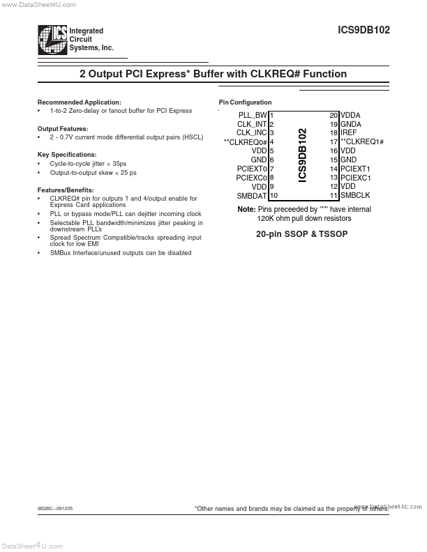
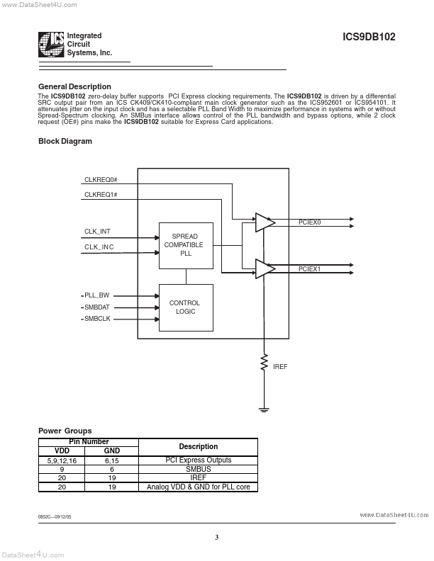
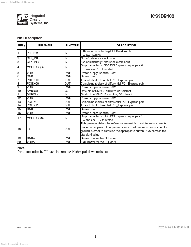
Datasheet4U Logo Datasheet4U.com

ICS9DB102 - 2 Output PCI Express Buffer

Description

PIN # 1 2 3 4 5 6 7 8 9 10 11 12 13 14 15 16 17 PLL_BW CLK_INT CLK_INC CLKREQ0# VDD GND PCIEXT0 PCIEXC0 VDD SMBDAT SMBCLK VDD PCIEXC1 PCIEXT1 GND VDD CLKREQ1# PIN NAME PIN TYPE IN IN IN IN PWR PWR OUT OUT PWR I/O IN PWR OUT OUT PWR PWR IN DESCRIPTION 3.3V input for selecting PLL

Features

  • 2 - 0.7V current mode differential output pairs (HSCL) Key Specifications:.
  • Cycle-to-cycle jitter < 35ps.
  • Output-to-output skew < 25 ps Features/Benefits:.
  • CLKREQ# pin for outputs 1 and 4/output enable for Express Card.

📥 Download Datasheet

Datasheet Details

Part number ICS9DB102
Manufacturer Integrated Circuit Systems
File Size 275.87 KB
Description 2 Output PCI Express Buffer
Datasheet download datasheet ICS9DB102 Datasheet
Other Datasheets by Integrated Circuit Systems

Full PDF Text Transcription

Click to expand full text
www.DataSheet4U.com Integrated Circuit Systems, Inc. ICS9DB102 2 Output PCI Express* Buffer with CLKREQ# Function Recommended Application: • 1-to-2 Zero-delay or fanout buffer for PCI Express Output Features: • 2 - 0.
Published: |