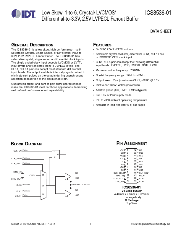
Low Skew, 1-to-6, Crystal/ LVCMOS/
ICS8536-01
Differential-to-3.3V, 2.5V LVPECL Fanout Buffer
DATA SHEET
GENERAL DESCRIPTION
The ICS8536-01 is a lo w skew, high performance 1-to-6
Selectable Crystal, Single-Ended, or Diff erential Input-to-
3.3V, 2.5V LVPECL Fanout Buffer. The ICS8536-01 has
selectable cr ystal, single ended or diff erential clock inputs.
The single ended cloc k input accepts LVCMOS or LVTTL
input levels and tr anslates them to LVPECL levels. The
CLK1, nCLK1 pair can accept most standard diff erential
input levels. The output enable is inter nally synchronized to
eliminate runt pulses on the outputs dur ing asynchronous
assertion/deassertion of the cloc k enable pin.
Guaranteed output and par t-to-part skew characteristics
make the ICS8536-01 ideal f or those applications demanding
well defined perf ormance and repeatability.
FEATURES
• Six 3.3V, 2.5V LVPECL outputs
• Selectable crystal oscillator, differential CLK1, nCLK1 pair
or LVCMOS/LVTTL clock input
• CLK1, nCLK pair can accept the f ollowing differential
input levels: LVPECL, LVDS, LVHSTL, SSTL, HCSL
• Maximum output frequency: 700MHz
• Crystal frequency range: 12MHz - 40MHz
• Output skew: 55ps (maximum) CLK1, nCLK1 @ 3.3V
• Part-to-part skew: 450ps (maximum)
• Additive phase jitter, RMS: 0.19ps (typical)
• Full 3.3V or 2.5V supply mode
• 0°C to 70°C ambient operating temperature
• Available in lead-free (RoHS 6) pac kages
BLOCK DIAGRAM
CLK_EN Pullup
CLK_SEL0 Pulldown
CLK_SEL1 Pulldown
XTAL_IN
XTAL_OUT
OSC
CLK0 Pulldown
CLK1 Pulldown
nCLK1 Pullup
00
01
1X
D
Q
LE
Q0
nQ0
6 LVPECL Outputs
Q5
nQ5
ICS8536-01 REVISION B AUGUST 17, 2012
1
PIN ASSIGNMENT
nQ2
Q2
VCC
nQ1
Q1
VEE
nQ0
Q0
CLK_SEL0
XTAL_IN
XTAL_OUT
CLK_EN
1
2
3
4
5
6
7
8
9
10
11
12
24 Q3
23 nQ3
22 VCC
21 Q4
20 nQ4
19 VCC
18 Q5
17 nQ5
16 CLK_SEL1
15 nCLK1
14 CLK1
13 CLK0
ICS8536-01
24-Lead TSSOP
4.40mm x 7.8mm x 0.925mm
package body
G Package
Top View
©2012 Integrated Device Technology, Inc.
http://www.Datasheet4U.com