• Part: ICS85411I
  • Description: 1-TO-2 DIFFERENTIAL-TO-LVDS FANOUT BUFFER
  • Manufacturer: Integrated Device Technology
  • Size: 321.39 KB
Download ICS85411I Datasheet PDF
Integrated Device Technology
ICS85411I
ICS85411I is 1-TO-2 DIFFERENTIAL-TO-LVDS FANOUT BUFFER manufactured by Integrated Device Technology.
LOW SKEW, 1-TO-2 DIFFERENTIAL-TOLVDS FANOUT BUFFER GENERAL DESCRIPTION 
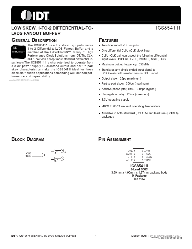
The ICS85411I is a low skew, high performance IC S 1-to-2 Differential-to-LVDS Fanout Buffer and a Hi Per Clock S™ member of the Hi Per Clock S™ family of High Performance Clock Solutions from IDT. The CLK, n CLK pair can accept most standard differential input levels.The ICS85411I is characterized to operate from a 3.3V power supply. Guaranteed output and par t-to-par t skew characteristics make the ICS85411I ideal for those clock distribution applications demanding well defined perfor mance and repeatability. .. Features - Two differential LVDS outputs - One differential CLK, n CLK clock input - CLK, n CLK pair can accept the following differential input levels: LVPECL, LVDS, LVHSTL, SSTL, HCSL - Maximum output frequency: 650MHz - Translates any single ended input signal to LVDS levels with resistor bias on n CLK input - Output skew: 25ps (maximum) - Part-to-part skew: 300ps (maximum) - Additive phase jitter, RMS: 0.05ps (typical) - Propagation delay: 2.5ns (maximum) - 3.3V operating supply - -40°C to 85°C ambient operating temperature - Available in both standard (Ro HS 5) and lead free (Ro HS 6) packages BLOCK DIAGRAM CLK n CLK Q0 n Q0 Q1 n Q1 PIN ASSIGNMENT Q0 n Q0 Q1 n Q1 1 2 3 4 8 7 6 5 VDD CLK n CLK GND 8-Lead SOIC 3.90mm x 4.90mm x 1.37mm package body M Package Top View IDT ™ / ICS™ DIFFERENTIAL-TO-LVDS FANOUT BUFFER ICS85411AMI REV. B NOVEMBER 7, 2007 ICS85411I LOW SKEW, 1-TO-2 DIFFERENTIAL-TO-LVDS FANOUT BUFFER TABLE 1. PIN DESCRIPTIONS Number 1, 2 3, 4 5 6 7 8 Name Q0, n Q0 Q1, n Q1 GND n CLK CLK VDD Type Output Output Power Input Input Power Pullup Description Differential output pair. LVDS interface levels. Differential output pair. LVDS interface levels. Power supply ground. Pulldown Inver ting differential clock input. Non-inver ting differential clock input. Positive supply pin. NOTE: Pullup and Pulldown refer to internal input resistors. See Table...