PRELIMINARY
LOW SKEW, DUAL, 1-TO-3 DIFFERENTIAL-TO-LVDS
FANOUT BUFFER
ICS854S013
General Description
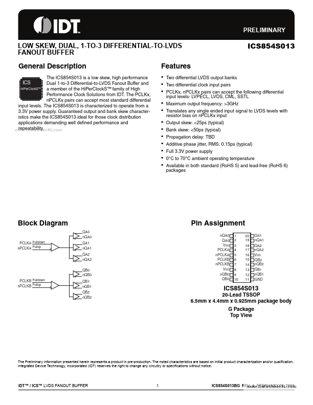
The ICS854S013 is a low skew, high performance
ICS Dual 1-to-3 Differential-to-LVDS Fanout Buffer and
HiPerClockS™ a member of the HiPerClockS™ family of High
Performance Clock Solutions from IDT. The PCLKx,
nPCLKx pairs can accept most standard differential
input levels. The ICS854S013 is characterized to operate from a
3.3V power supply. Guaranteed output and bank skew character-
istics make the ICS854S013 ideal for those clock distribution
applications demanding well defined performance and
wwrewp.eDaatatabSilhitey.et4U.com
Features
• Two differential LVDS output banks
• Two differential clock input pairs
• PCLKx, nPCLKx pairs can accept the following differential
input levels: LVPECL, LVDS, CML, SSTL
• Maximum output frequency: >3GHz
• Translates any single ended input signal to LVDS levels with
resistor bias on nPCLKx input
• Output skew: <25ps (typical)
• Bank skew: <50ps (typical)
• Propagation delay: TBD
• Additive phase jitter, RMS: 0.15ps (typical)
• Full 3.3V power supply
• 0°C to 70°C ambient operating temperature
• Available in both standard (RoHS 5) and lead-free (RoHS 6)
packages
Block Diagram
PCLKA Pulldown
nPCLKA Pullup
PCLKB Pulldown
nPCLKB Pullup
QA0
nQA0
QA1
nQA1
QA2
nQA2
QB0
nQB0
QB1
nQB1
QB2
nQB2
Pin Assignment
nQA0
QA0
VDD
PCLKA
nPCLKA
PCLKB
nPCLKB
VDD
nQB0
QB0
1
2
3
4
5
6
7
8
9
10
20 QA1
19 nQA1
18 QA2
17 nQA2
16 VDD
15 QB2
14 nQB2
13 QB1
12 nQB1
11 GND
ICS854S013
20-Lead TSSOP
6.5mm x 4.4mm x 0.925mm package body
G Package
Top View
The Preliminary Information presented herein represents a product in pre-production. The noted characteristics are based on initial product characterization and/or qualification.
Integrated Device Technology, Incorporated (IDT) reserves the right to change any circuitry or specifications without notice.
IDT™ / ICS™ LVDS FANOUT BUFFER
1 ICS854S013BG REV. A FEBRUARY 26, 2008