ICS854S058I Description
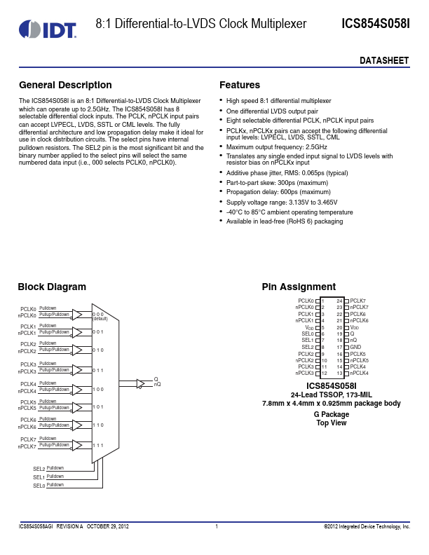
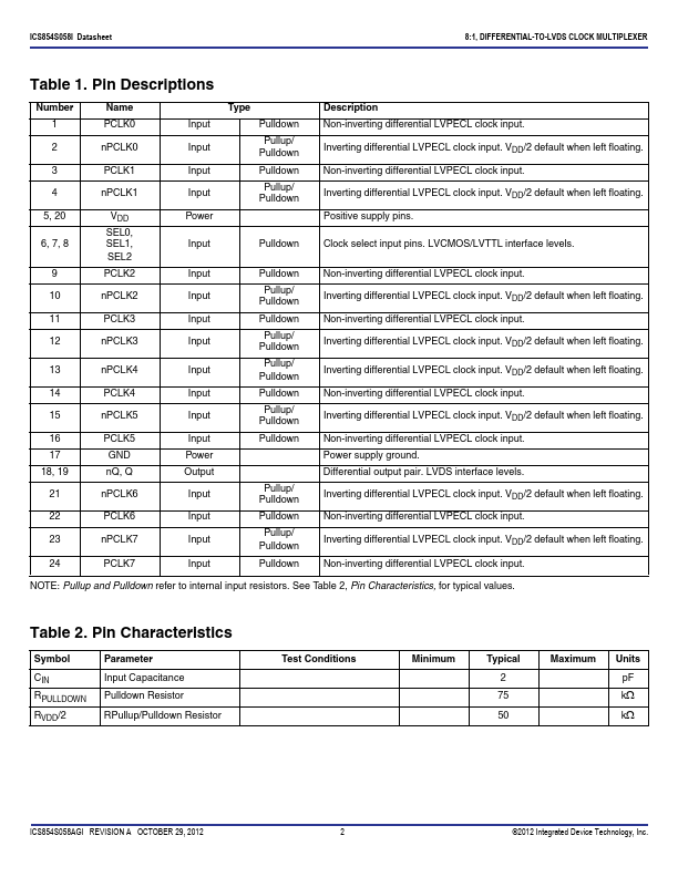
The ICS854S058I is an 8:1 Differential-to-LVDS Clock Multiplexer which can operate up to 2.5GHz. The ICS854S058I has 8 selectable differential clock inputs. The PCLK, nPCLK input pairs can accept LVPECL, LVDS, SSTL or CML levels.
ICS854S058I Key Features
- High speed 8:1 differential multiplexer
- One differential LVDS output pair
- Eight selectable differential PCLK, nPCLK input pairs
- PCLKx, nPCLKx pairs can accept the following differential
- Maximum output frequency: 2.5GHz
- Additive phase jitter, RMS: 0.065ps (typical)
- Part-to-part skew: 300ps (maximum)
- Propagation delay: 600ps (maximum)
- Supply voltage range: 3.135V to 3.465V
- 40°C to 85°C ambient operating temperature