Datasheet4U Logo Datasheet4U.com

IS49NLS18160 - Separate I/O RLDRAM 2 Memory

Download the IS49NLS18160 datasheet PDF (IS49NLS93200 included). The manufacturer datasheet provides complete specifications, pinout details, electrical characteristics, and typical applications for separate i/o rldram 2 memory.

Description

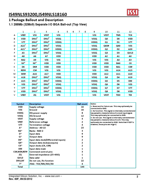
1.1 288Mb (32Mx9) Separate I/O BGA Ball-out (Top View) 123 4 5678 9 10 11 12 A VREF B VDD VSS DNU3 VEXT DNU3 VSS VSSQ VSS VEXT TMS TCK VSSQ Q0 D0 VDD C VTT DNU3 DNU3 VDDQ VDDQ Q1 D1 VTT D A221 DNU3 DNU3 VSSQ VSSQ QK0# QK0 VSS E A211 DNU3 DNU3 VDDQ VDDQ Q2 D2 A20

📥 Download Datasheet

Note: The manufacturer provides a single datasheet file (IS49NLS93200-IntegratedSiliconSolution.pdf) that lists specifications for multiple related part numbers.
Other Datasheets by Integrated Silicon Solution

Full PDF Text Transcription

Click to expand full text
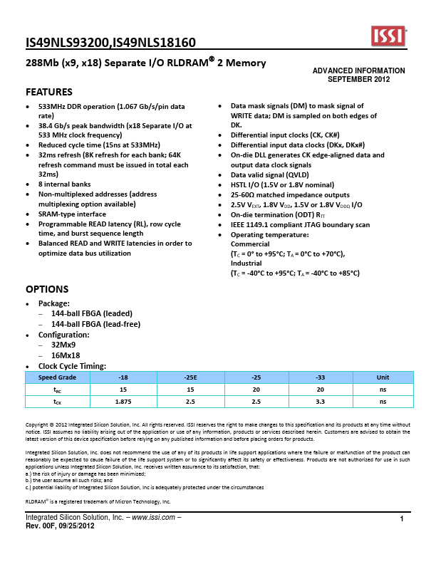
IS49NLS93200,IS49NLS18160 288Mb (x9, x18) Separate I/O RLDRAM® 2 Memory FEATURES ADVANCED INFORMATION SEPTEMBER 2012 • 533MHz DDR operation (1.067 Gb/s/pin data rate) • 38.4 Gb/s peak bandwidth (x18 Separate I/O at 533 MHz clock frequency) • Reduced cycle time (15ns at 533MHz) • 32ms refresh (8K refresh for each bank; 64K refresh command must be issued in total each 32ms) • 8 internal banks • Non-multiplexed addresses (address multiplexing option available) • SRAM-type interface • Programmable READ latency (RL), row cycle time, and burst sequence length • Balanced READ and WRITE latencies in order to optimize data bus utilization • Data mask signals (DM) to mask signal of WRITE data; DM is sampled on both edges of DK.
Published: |