IS49NLS96400A Description
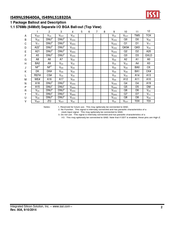
1.1 576Mb (64Mx9) Separate I/O BGA Ball-out (Top View) 1 2 3 4 5678 A VREF VSS VEXT VSS B VDD DNU3 DNU3 VSSQ C VTT DNU3 DNU3 VDDQ D A221 DNU3 DNU3 VSSQ E A21 DNU3 DNU3 VDDQ F A5 DNU3 DNU3 VSSQ G A8 A6 A7 VDD H BA2 A9 VSS VSS.
IS49NLS96400A Key Features
- 533MHz DDR operation (1.067 Gb/s/pin data rate)
- 38.4Gb/s peak bandwidth (x18 at 533 MHz clock
- Reduced cycle time (15ns at 533MHz)
- 32ms refresh (16K refresh for each bank; 128K
- 8 internal banks
- Non-multiplexed addresses (address multiplexing option available)
- SRAM-type interface
- Programmable READ latency (RL), row cycle time, and burst sequence length
- Balanced READ and WRITE latencies in order to optimize data bus utilization
- Data mask signals (DM) to mask signal of WRITE data; DM is sampled on both edges of DK