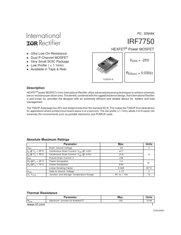
IRF7750
Electrical Characteristics @ TJ = 25°C (unless otherwise specified)
Parameter
Min. Typ. Max. Units
Conditions
V(BR)DSS Drain-to-Source Breakdown Voltage
-20 ––– ––– V VGS = 0V, ID = -250µA
∆V(BR)DSS/∆TJ Breakdown Voltage Temp. Coefficient
RDS(on)
Static Drain-to-Source On-Resistance
––– 0.012 ––– V/°C
––– ––– 0.030
––– ––– 0.055 Ω
Reference to 25°C, ID = -1mA
VGS = -4.5V, ID = -4.7A
VGS = -2.5V, ID = -3.8A
VGS(th)
Gate Threshold Voltage
-0.45 ––– -1.2 V VDS = VGS, ID = -250µA
gfs Forward Transconductance
11 ––– ––– S VDS = -10V, ID = -4.7A
IDSS Drain-to-Source Leakage Current
––– ––– -1.0
––– ––– -25
µA
VDS = -20V, VGS = 0V
VDS = -16V, VGS = 0V, TJ = 70°C
IGSS
Gate-to-Source Forward Leakage
Gate-to-Source Reverse Leakage
––– ––– -100 nA VGS = -12V
––– ––– 100
VGS = 12V
Qg Total Gate Charge
––– 26 39
ID = -4.7A
Qgs Gate-to-Source Charge
––– 3.9 5.8 nC VDS = -16V
Qgd Gate-to-Drain ("Miller") Charge
––– 8.0 12
VGS = -5.0V
td(on)
Turn-On Delay Time
––– 15 –––
VDD = -10V
tr
td(off)
Rise Time
Turn-Off Delay Time
––– 54 ––– ns ID = -1.0A
––– 180 –––
RD = 10Ω
tf Fall Time
––– 210 –––
RG = 24Ω
Ciss Input Capacitance
––– 1700 –––
VGS = 0V
Coss
Output Capacitance
––– 380 ––– pF VDS = -15V
Crss Reverse Transfer Capacitance
––– 270 –––
ƒ = 1.0MHz
Source-Drain Ratings and Characteristics
Parameter
IS Continuous Source Current
(Body Diode)
ISM Pulsed Source Current
(Body Diode)
VSD Diode Forward Voltage
trr Reverse Recovery Time
Qrr Reverse RecoveryCharge
Min.
–––
–––
–––
–––
–––
Typ. Max.
––– -1.0
––– -38
––– -1.2
26 39
16 24
Units
A
V
ns
nC
Conditions
MOSFET symbol
D
showing the
integral reverse
G
p-n junction diode.
S
TJ = 25°C, IS = -1.0A, VGS = 0V
TJ = 25°C, IF = -1.0A
di/dt = 100A/µs
Notes:
Repetitive rating; pulse width limited by
max. junction temperature.
Pulse width ≤ 300µs; duty cycle ≤ 2%.
When mounted on 1 inch square copper board, t<10 sec
2 www.irf.com