The following content is an automatically extracted verbatim text
from the original manufacturer datasheet and is provided for reference purposes only.
View original datasheet text
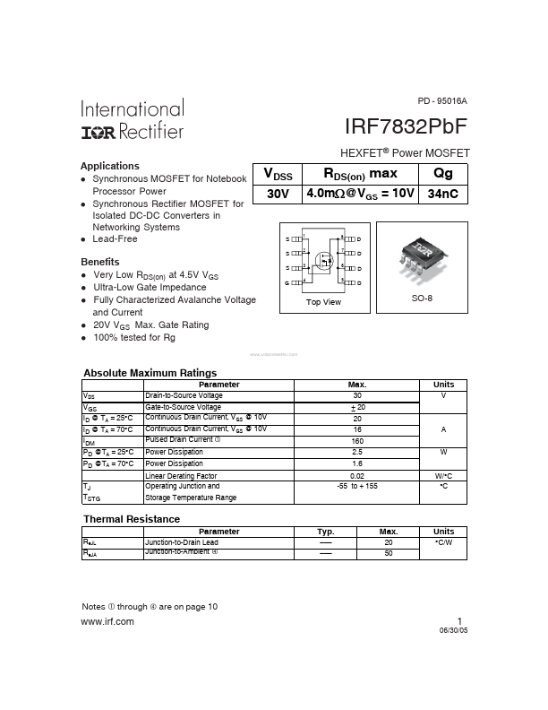
PD - 95016A
IRF7832PbF
HEXFET® Power MOSFET
Applications l Synchronous MOSFET for Notebook Processor Power l Synchronous Rectifier MOSFET for Isolated DC-DC Converters in Networking Systems l Lead-Free Benefits l Very Low RDS(on) at 4.5V VGS l Ultra-Low Gate Impedance l Fully Characterized Avalanche Voltage and Current l 20V VGS Max. Gate Rating l 100% tested for Rg
VDSS
30V
4.0m:@VGS = 10V
1 2 3 4 8 7
RDS(on) max
Qg
34nC
S S S G
A A D D D D
6 5
Top View
SO-8
www.DataSheet4U.com
Absolute Maximum Ratings
Parameter
VDS VGS ID @ TA = 25°C ID @ TA = 70°C IDM PD @TA = 25°C PD @TA = 70°C TJ TSTG Drain-to-Source Voltage Gate-to-Source Voltage Continuous Drain Current, VGS @ 10V Continuous Drain Current, VGS @ 10V Pulsed Drain Current
Max.
30 ± 20 20 16 160 2.5 1.6 0.
 IRF7832PBF Datasheet