Datasheet4U Logo Datasheet4U.com

CD4043BMS - CMOS Quad 3 State R/S Latche

Datasheet Summary

Description

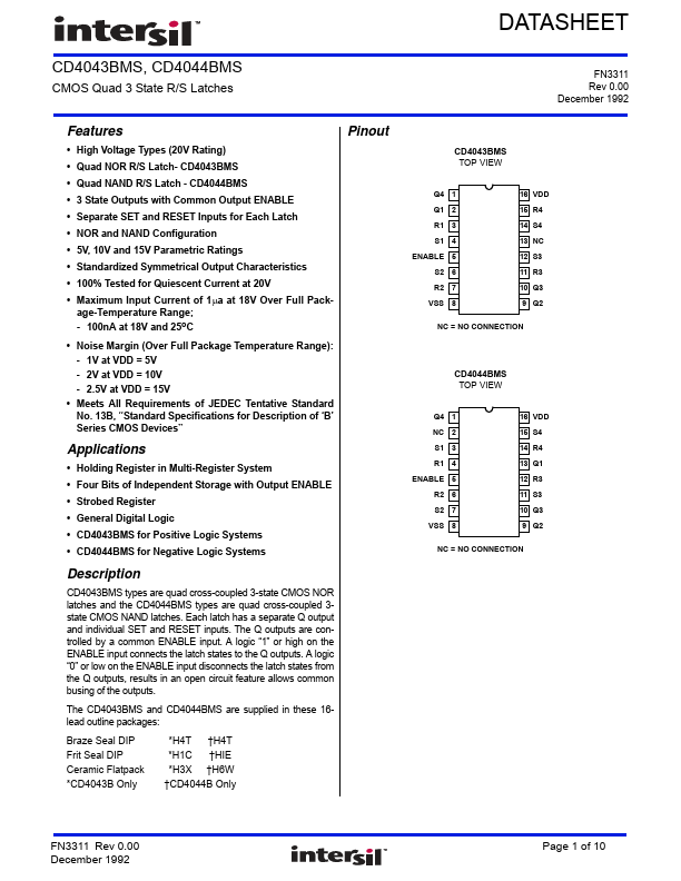
of ‘B’ Series CMOS Devices” Pinout Applications Holding Register in Multi-Register System Four Bits of Independent Storage with Output ENABLE Strobed Register General Digital Logic CD4043BMS for Positive Logic Systems CD4044BMS for Negati

Features

  • High Voltage Types (20V Rating).
  • Quad NOR R/S Latch- CD4043BMS.
  • Quad NAND R/S Latch - CD4044BMS.
  • 3 State Outputs with Common Output ENABLE.
  • Separate SET and RESET Inputs for Each Latch.
  • NOR and NAND Configuration.
  • 5V, 10V and 15V Parametric Ratings.
  • Standardized Symmetrical Output Characteristics.
  • 100% Tested for Quiescent Current at 20V.
  • Maximum Input Current of 1a at 18V Over Full Package-Temperature Ra.

📥 Download Datasheet

Datasheet preview – CD4043BMS

Datasheet Details

Part number CD4043BMS
Manufacturer Intersil Corporation
File Size 391.08 KB
Description CMOS Quad 3 State R/S Latche
Datasheet download datasheet CD4043BMS Datasheet
Additional preview pages of the CD4043BMS datasheet.
Other Datasheets by Intersil Corporation

Full PDF Text Transcription

Click to expand full text
DATASHEET CD4043BMS, CD4044BMS CMOS Quad 3 State R/S Latches FN3311 Rev 0.00 December 1992 Features • High Voltage Types (20V Rating) • Quad NOR R/S Latch- CD4043BMS • Quad NAND R/S Latch - CD4044BMS • 3 State Outputs with Common Output ENABLE • Separate SET and RESET Inputs for Each Latch • NOR and NAND Configuration • 5V, 10V and 15V Parametric Ratings • Standardized Symmetrical Output Characteristics • 100% Tested for Quiescent Current at 20V • Maximum Input Current of 1a at 18V Over Full Package-Temperature Range; - 100nA at 18V and 25oC • Noise Margin (Over Full Package Temperature Range): - 1V at VDD = 5V - 2V at VDD = 10V - 2.5V at VDD = 15V • Meets All Requirements of JEDEC Tentative Standard No.
Published: |