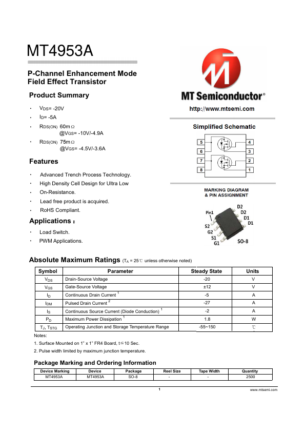
The following content is an automatically extracted verbatim text
from the original manufacturer datasheet and is provided for reference purposes only.
View original datasheet text
MT4953A
P-Channel Enhancement Mo de
Field Effect Transistor
Product Summary
VDS= -20V ID= -5A RDS(ON) 60m
@VGS= -10V/-4.9A RDS(ON) 75m
@VGS= -4.5V/-3.6A
Features
Advanced Trench Process Technology. High Density Cell Design for Ultra Low On-Resistance. Lead free product is acquired. RoHS Compliant.
Applications ˖
Load Switch. PWM Applications.
Absolute Maximum Ratings (TA = 25 unless otherwise noted)
Symbol
Parameter
VDS VGS ID IDM IS PD
TJ, TSTG
Drain-Source Voltage
Gate-Source Voltage Continuous Drain Current 1 Pulsed Drain Current 2 Continuous Source Current (Diode Conduction) 1 Maximum Power Dissipation 1
Operating Junction and Storage Temperature Range
Notes:
1. Surface Mounted on 1” x 1” FR4 Board, t 10 Sec.
2.